Datasheet Summary
3PEAK
Features
- Low Offset Voltage: 100μV Maximum
- Low Drift: ±0.9μV/°C
- High EMIRR: 84dB at 900MHz
- Low Noise: 19 nV/√Hz(f= 1kHz)
- Wide Input Voltage Range: 0 to ±14V
- Wide Supply Range: ±1.35V to ±18V
- Low Input Bias Current: 40pA Typical
- Below-Ground (V-) Input Capability to -0.3V
- Rail-to-Rail Output Voltage Range
- Unit Gain Stable
- - 40°C to 125°C Operation Range
- Robust 3kV
- HBM and 2kV
- CDM ESD Rating
- Direct or Update Replacement for OP07C,OP07D and OP37
Applications
- Wireless Base Station Control Circuits
- Optical network Control Circuits
- I/V Converter
- Temperature Measurements
- Strain Gage Amplifier
- Medical Instrumentation
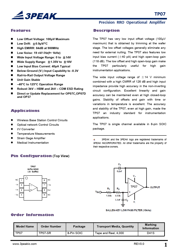
Pin Configuration (Top...