Datasheet4U Logo Datasheet4U.com

AVR201628 - DDR2 SDRAM

Download the AVR201628 datasheet PDF. This datasheet also covers the AVR201628-A variant, as both devices belong to the same ddr2 sdram family and are provided as variant models within a single manufacturer datasheet.

Description

The DDR2 SDRAM uses a double data rate architecture to achieve high-speed operation.

The double data rate architecture is essentially a 4n-prefetch architecture, with an interface designed to transfer two data words per clock cycle at the I/O balls.

Features

  • VDD = +1.8V ±0.1V, VDDQ = +1.8V ±0.1V.
  • JEDEC-standard 1.8V I/O (SSTL_18-compatible).
  • Differential data strobe (DQS, DQS#) option.
  • 4n-bit prefetch architecture.
  • Duplicate output strobe (RDQS) option for x8.
  • DLL to align DQ and DQS transitions with CK.
  • 8 internal banks for concurrent operation.
  • Programmable CAS latency (CL).
  • Posted CAS additive latency (AL).
  • WRITE latency = READ latency - 1 tCK.
  • Pro.

📥 Download Datasheet

Note: The manufacturer provides a single datasheet file (AVR201628-A-LINK.pdf) that lists specifications for multiple related part numbers.

Datasheet Details

Part number AVR201628
Manufacturer A-LINK
File Size 8.12 MB
Description DDR2 SDRAM
Datasheet download datasheet AVR201628 Datasheet

Full PDF Text Transcription (Reference)

The following content is an automatically extracted verbatim text from the original manufacturer datasheet and is provided for reference purposes only.

View original datasheet text
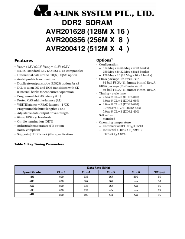
DDR2 SDRAM AVR201628 (128M X 16 ) AVR200856 (256M X 8 ) AVR200412 (512M X 4 ) Features • VDD = +1.8V ±0.1V, VDDQ = +1.8V ±0.1V • JEDEC-standard 1.
Published: |