ADESTO AT25DN512C
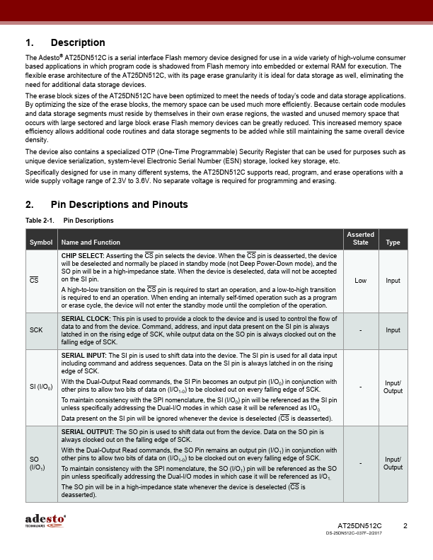
AT25DN512C is a serial interface Flash memory device designed for use in a wide variety of high-volume consumer based applications in which program code is shadowed from Flash memory into embedded or external RAM for execution. The flexible erase architecture of the AT25DN512C, with its page erase granularity it is ideal for data storage as well, eliminating the need for additional data storage devices. The erase block sizes of the AT25DN512C have been optimized to meet the needs of today's code and data storage applications.| Part No. | AT25DN512C |
|---|---|
| Datasheet | AT25DN512C Download |
| Manufacturer |  ADESTO |
| Description | 512-Kbit 2.3V Minimum SPI Serial Flash Memory |
| Buy | Stock & Price |
FEATURES
● Single 2.3V - 3.6V Supply● Serial Peripheral Interface (SPI) Compatible Supports SPI Modes 0 and 3 Supports Dual Output Read
● 85MHz Maximum Operating Frequency
● Clock-to-Output (tV) of 7 ns
● Flexible, Optimized Erase Architecture for Code + Data Storage
APPLICATIONS
● Uniform 256-Byte Page erase● Uniform 4-Kbyte Block Erase
● Uniform 32-Kbyte Block Erase
● Full Chip Erase
● Hardware Controlled Locking of Protected Sectors via WP Pin
● 128-Byte Programmable OTP Security Register
● Flexible Programming
●
● Byte/Page Program (1 to 256 Bytes)
● Fast Program and Erase Times
● 1.5ms Typical Page Program (256 Bytes) Time
● 50ms Typical 4-Kbyte Block Erase Time
● 400ms Typical 32-Kbyte Block Erase Time
● Automatic Checking and Reporting of Erase/Program Failures
● Software Controlled Reset
● JEDEC Standard Manufacturer and Device ID Read Methodology
● Low Power Dissipation
● 200nA Ultra Deep Power Down current (Typical) 5µA Deep Power-Down Current (Typical) 25uA Standby current...