AGMSEMI AGM628MAP
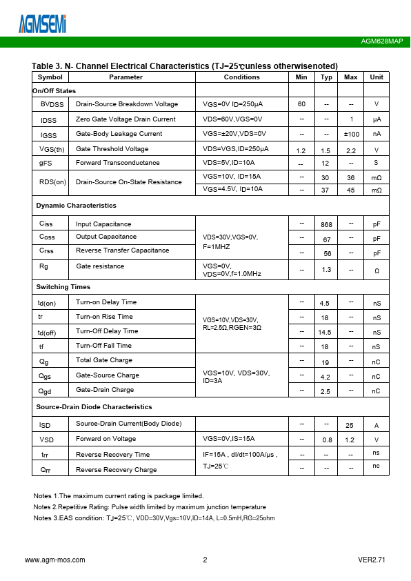
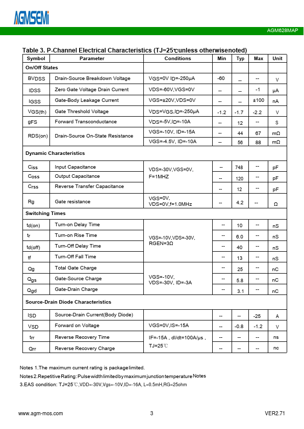
The AGM628MAP combines advanced trench MOSFET technology with a low resistance package to provide extremely low RDS(ON) . This device is ideal for load switch and battery protection applications.| Part No. | AGM628MAP |
|---|---|
| Datasheet | AGM628MAP Download |
| Manufacturer |  AGMSEMI |
| Description | MOSFET |
| Buy | Stock & Price |
GENERAL DESCRIPTION
●FEATURES
● Advance high cell density Trench technology● Low RDS(ON) to minimize conductive loss
●Low Gate Charge for fast switching
●Low Thermal resistance
●100% Avalanche tested
●100% DVDS tested
● Application
●MB/VGA Vcore
●SMPS 2nd Synchronous Rectifier
●POL application
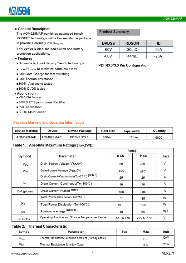
●BLDC Motor driver Product Summary BVDSS 60V -60V RDSON 30mΩ 44mΩ ID 25A -25A PDFN3.3*3.3 Pin Configuration Package Marking and Ordering Information Device Marking Device AGM628MAP AGM628MAP Device Package PDFN3.3*3.3 Reel Size 330mm Tape width 12mm Quantity 5000 Table 1.
ABSOLUTE MAXIMUM RATINGS
(TA=25℃) Symbol VDS VGS ID IDM (pluse) PD EAS TJ,TSTG Parameter Drain-Source Voltage (VGS=0V) Gate-Source Voltage (VDS=0V) Drain Current-Continuous(Tc=25℃) (Note 1) Drain Current-Continuous(Tc=100℃) Drain Current-Pulsed (Note 2) Total Power Dissipation(Tc=25℃) Total Power Dissipation(Tc=100℃) Avalanche energy (Note 3) Operating Junction and Storage Temperature Range Rating N-Ch P-Ch 60 ±20 25 16 100 35 13.8 49 -55 To 150 -60 ±20 -25 -16 -100 35 13.8 65 -55 To 150 Units V V A A A W W mJ ℃ Table 2.