FEATURES
Output Frequency Range: 74.17582MHz / 74.25MHz (Selectable) Input Frequency: 27MHz DESCRIPTION
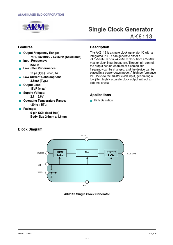
Through pin control, the output can be enabled or disabled, the frequency can be changed, and the device can be placed in a power-down mode. A high performance PLL locks to the master clock input, generating a low jitter, highly accurate clock output without an external crystal. Low Jitter Performance: 15 ps (Typ.) Period, 1σ Low Current Consumption: 3.8mA (Typ.) Output Load: 15pF (max.) Supply Voltage: 2.7 – 3.6V Operating Temperature Range: -20 to +85℃ Package: 6-pin SON (lead-free) Body Size 2.6mm x 1.6mm APPLICATIONS
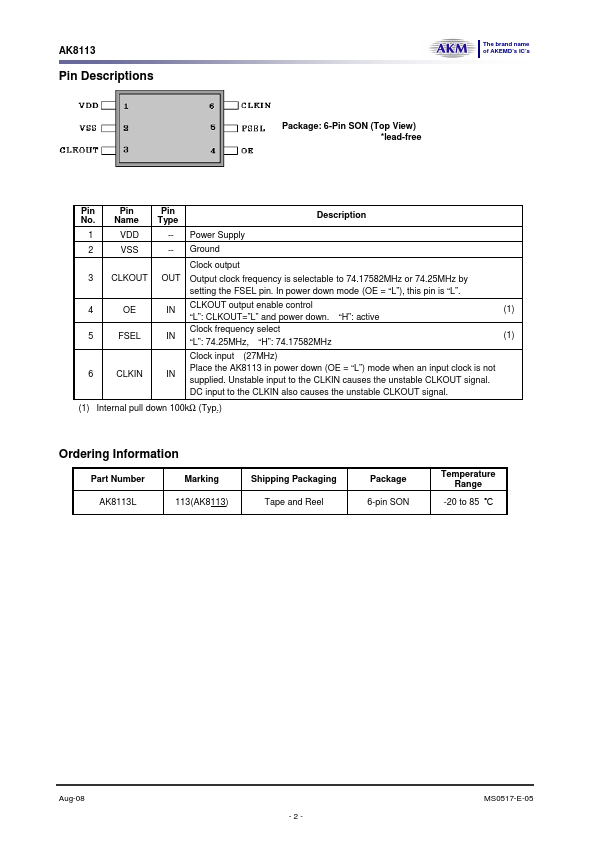
High Definition Block Diagram AK8113 Single Clock Generator MS0517-E-05 -1- Aug-08 AK8113 The brand name of AKEMD’s IC’s Pin Descriptions Package: 6-Pin SON (Top View) *lead-free Pin No. 1 2 3 Pin Name VDD VSS CLKOUT Pin Type --OUT Power Supply Ground Clock output DESCRIPTION
Output clock frequency is selectable to 74.17582MHz or 74.25MHz by setting the FSEL pin. In power down mode (OE = “L”), this pin is “L”. Asahi Kasei Microdevices