AK8181F
AK8181F is 3.3V LVPECL 1:4 Clock Fanout Buffer manufactured by Asahi Kasei Microdevices.
Features
Four differential 3.3V LVDS outputs Selectable differential PCLK0p/n or LVPECL clock inputs PCLK0p/n pair can accept the following differential input levels; LVDS, LVPECL, LVHSTL, SSTL, HCSL PCLK1p/n supports the following input types; LVPECL, CML, SSTL Clock output frequency up to 650MHz Translates any single-ended input signal to 3.3V LVDS levels with resistor bias on PCLK0n input Output skew : 30ps (maximum) Part-to-part skew : 600ps (maximum) Propagation delay : 2.5ns (maximum) Operating Temperature Range: -40 to +85℃ Package: 20-pin TSSOP (Pb free) Pin patible with ICS8543I
Description
The AK8181F is a member of AKM’s LVDS clock fanout buffer family designed for tele, networking and puter applications, requiring a range of clocks with high performance and low skew. The AK8181F distributes 4 buffered clocks. AK8181F are derived from AKM’s long-termexperienced clock device technology, and enable clock output to perform low skew. The AK8181F is available in a 20-pin TSSOP package.
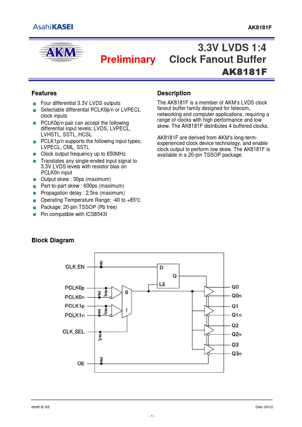
Block Diagram draft-E-02 -1-
Dec-2012 http://..
Pin Descriptions
Package: 20-Pin TSSOP(Top View)
Pullup down --Negative power supply Synchronizing clock output enable (LVCMOS/LVTTL) Pin is connected to VDD by internal resistor. (typ. 51kΩ High (Open): clock outputs follow clock input. Low: Q outputs are forced low, Qn outputs are forced high. CLK Select Input (LVCMOS/LVTTL) Pin is connected to VSS by internal resistor. (typ. 51kΩ High: selects PCLK1p/n inputs Low (Open): selects PCLK0p/n inputs Non-inverting differential clock input 4 PCLK0p IN Pull down Pin is connected to VSS by internal resistor. (typ. 51kΩ
- When using PCLK1 input (CLK_SEL=High), it should be connected to VSS or opened. Inverting differential clock input 5 PCLK0n IN Pull up Pin is connected to VDD by internal resistor. (typ. 51kΩ
- When using PCLK1 input (CLK_SEL=High), it should be connected to VDD or opened. Non-inverting differential LVPECL clock input 6 PCLK1p IN Pull down Pin is...