AK8181G
AK8181G is 3.3V LVDS 1:4 Clock Fanout Buffer manufactured by Asahi Kasei Microdevices.
Features
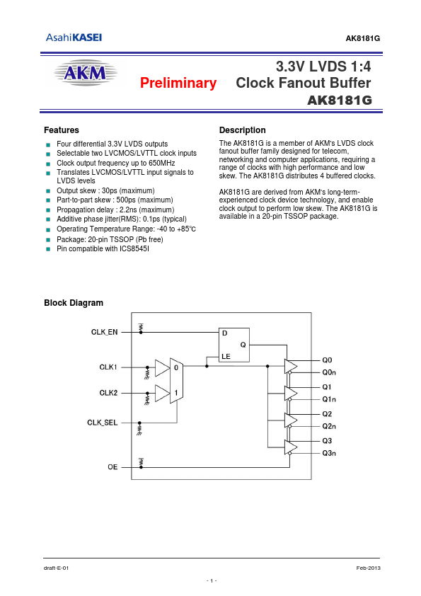
Four differential 3.3V LVDS outputs Selectable two LVCMOS/LVTTL clock inputs Clock output frequency up to 650MHz Translates LVCMOS/LVTTL input signals to LVDS levels Output skew : 30ps (maximum) Part-to-part skew : 500ps (maximum) Propagation delay : 2.2ns (maximum) Additive phase jitter(RMS): 0.1ps (typical) Operating Temperature Range: -40 to +85℃ Package: 20-pin TSSOP (Pb free) Pin patible with ICS8545I
Description
The AK8181G is a member of AKM’s LVDS clock fanout buffer family designed for tele, networking and puter applications, requiring a range of clocks with high performance and low skew. The AK8181G distributes 4 buffered clocks. AK8181G are derived from AKM’s long-termexperienced clock device technology, and enable clock output to perform low skew. The AK8181G is available in a 20-pin TSSOP package.
Block Diagram draft-E-01 -1-
Feb-2013 http://..
Pin Descriptions
Package: 20-Pin TSSOP(Top View)
Pin No. 1 Pin Name VSS Pin Type PWR Pullup down --Negative power supply Synchronizing clock output enable (LVCMOS/LVTTL) Pin is connected to VDD by internal resistor. (typ. 51kΩ High (Open): clock outputs follow clock input. Low: Q outputs are forced low, Qn outputs are forced high. CLK Select Input (LVCMOS/LVTTL) Pin is connected to VSS by internal resistor. (typ. 51kΩ High: selects CLK2 input Low (Open): selects CLK1 input 4 5 6 7 8 9 10 11, 12 13 14, 15 16, 17 18 19, 20 CLK1 NC CLK2 NC OE VSS VDD Q3n, Q3 VSS Q2n, Q2 Q1n, Q1 VDD Q0n, Q0 IN -IN -IN PWR PWR OUT PWR OUT OUT PWR OUT Pull down --Pull down --Pull up ----------------Single-ended clock input Pin is connected to VSS by internal resistor. (typ. 51kΩ No connect Single-ended clock input Pin is connected to VSS by internal resistor. (typ. 51kΩ No connect Output enable. Controls enabling and disabling of outputs Q0, Q0n through Q3, Q3n. Pin is connected to VDD by internal resistor. (typ. 51kΩ Negative power supply Positive power supply Differential clock output (LVDS) Negative...