Datasheet4U Logo Datasheet4U.com

M1489 - 486 PCI Chip Set

Download the M1489 datasheet PDF. This datasheet also covers the M1487 variant, as both devices belong to the same 486 pci chip set family and are provided as variant models within a single manufacturer datasheet.

Description

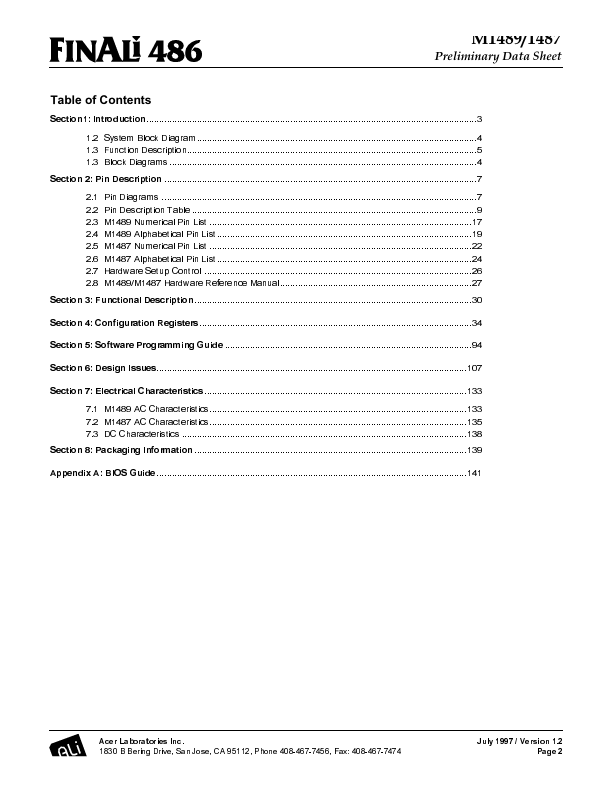
1.3 Block Diagrams 4 Section 2: Pin Description 7 2.1 Pin Diagrams 7 2.2 Pin Description Table 9 2.3 M1489 Numerical Pin List 17 2.4 M1489 Alphabetical Pin List 19 2.5 M1487 Numerical Pin List 22 2.6 M1487 Alphabetical Pin List 24 2.7 Hardware Setup Control 26 2.8 M1489/M1487 Hardware Reference Man

Features

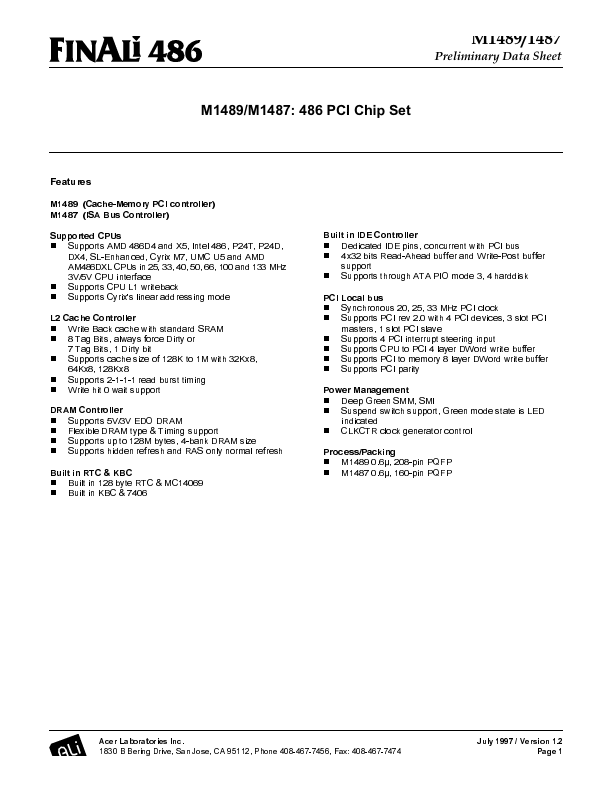
  • M1489 (Cache-Memory PCI controller) M1487 (ISA Bus Controller) Supported CPUs T Supports AMD 486D4 and X5, Intel 486, P24T, P24D, DX4, SL-Enhanced, Cyrix M7, UMC U5 and AMD AM486DXL CPUs in 25, 33, 40, 50, 66, 100 and 133 MHz 3V/5V CPU interface T Supports CPU L1 writeback T Supports Cyrix's linear addressing mode L2 Cache Controller T Write Back cache with standard SRAM T 8 Tag Bits, always force Dirty or 7 Tag Bits, 1 Dirty bit T Supports cache size of 128K to 1M with 32Kx8, 64Kx8, 128Kx8 T Su.

📥 Download Datasheet

Note: The manufacturer provides a single datasheet file (M1487_ALi.pdf) that lists specifications for multiple related part numbers.

Datasheet Details

Part number M1489
Manufacturer ALi
File Size 3.35 MB
Description 486 PCI Chip Set
Datasheet download datasheet M1489 Datasheet

Full PDF Text Transcription (Reference)

The following content is an automatically extracted verbatim text from the original manufacturer datasheet and is provided for reference purposes only.

View original datasheet text
0 3UHOLPLQDU'DWD6KHHW M1489/M1487: 486 PCI Chip Set Features M1489 (Cache-Memory PCI controller) M1487 (ISA Bus Controller) Supported CPUs T Supports AMD 486D4 and X5, Intel 486, P24T, P24D, DX4, SL-Enhanced, Cyrix M7, UMC U5 and AMD AM486DXL CPUs in 25, 33, 40, 50, 66, 100 and 133 MHz 3V/5V CPU interface T Supports CPU L1 writeback T Supports Cyrix's linear addressing mode L2 Cache Controller T Write Back cache with standard SRAM T 8 Tag Bits, always force Dirty or 7 Tag Bits, 1 Dirty bit T Supports cache size of 128K to 1M with 32Kx8, 64Kx8, 128Kx8 T Supports 2-1-1-1 read burst timing T Write hit 0 wait support DRAM Controller T Supports 5V/3V EDO DRAM T Flexible DRAM type & Timing support T Supports up to 128M bytes, 4-bank DRAM size T Supports hidden refresh and RAS only no
Datasheet originally released: |