GENERAL DESCRIPTION
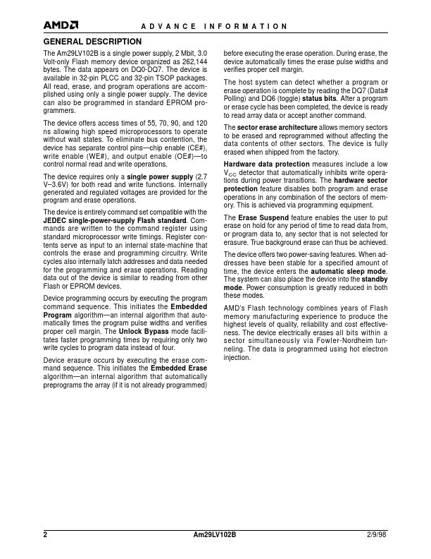
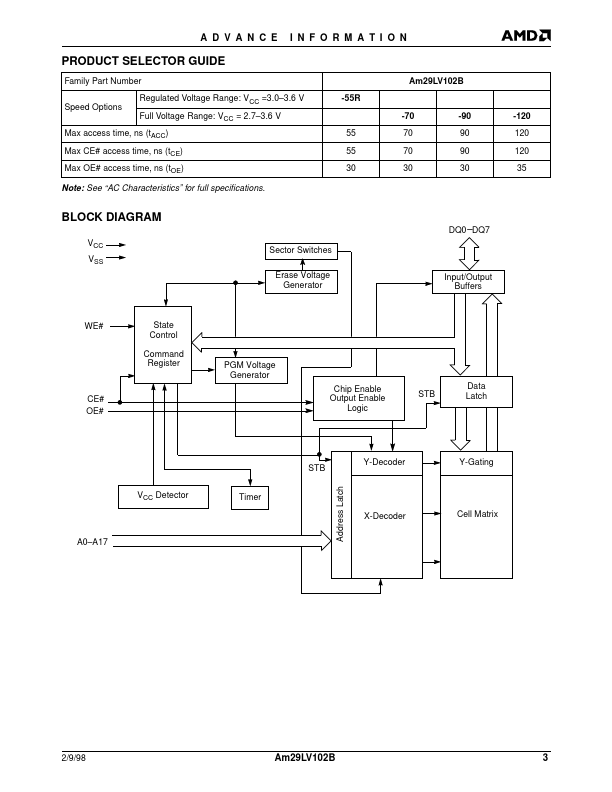
The data appears on DQ0-DQ7. All read, erase, and program operations are accomplished using only a single power supply. The device can also be programmed in standard EPROM programmers. The device offers access times of 55, 70, 90, and 120 ns allowing high speed microprocessors to operate without wait states. To eliminate bus contention, the device has separate control pins—chip enable (CE#), write enable (WE#), and output enable (OE#)—to control normal read and write operations. The device requires only a single power supply (2.7 V–3.6V) for both read and write functions. Internally generated and regulated voltages are provided for the program and erase operations. The device is entirely command set compatible with the JEDEC single-power-supply Flash standard. Commands are written to the command register using standard microprocessor write timings. Register contents serve as input to an internal state-machine that controls the erase and programming circuitry. Write cycles also internally latch addresses and data needed for the programming and erase operations. AMD