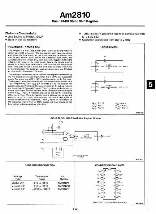
DESCRIPTION
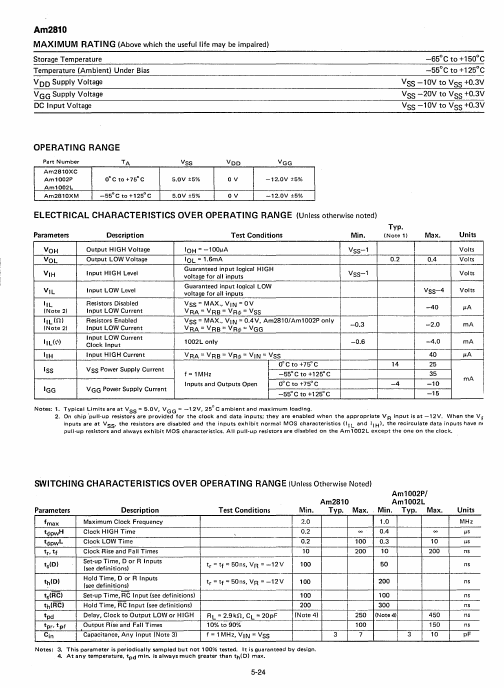
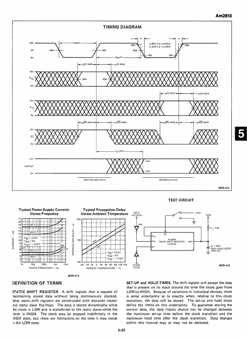
Data at the inputs must be steady for a set-up time before and a hold time after this clock transition. Since data storage is static, the clock may be halted indefinitely in the HIGH state. When RC is LOW, data is accepted on the Rin input; when RC is HIGH, data is accepted on the Din input. The inputs to the registers have built-in pull-up resistors to provide total TTL compatibility. The VRA pin controls the pull-up resistors for register A Din and RC inputs. The VRB pin controls the pull-up resistors for the register B Din and RC inputs. The VRct> pin controls the resistor on the clock input to both registers. When the resistor control pins are tied to VGG (-12V), the resistors are enabled and pull the inputs they affect up to VSS. When the resistor control pins are tied to VSS the resistors are all very high impedance and the inputs they affect all exhibit normal MOS characteristics. The Rin inputs are intended to be the ~'recirculate inputs from an MOS output ant:! these inputs do not have pull-up resistors associated with them. AMD