DESCRIPTION
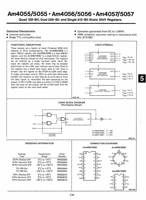
These devices are a family of static P-channel MOS shift registers in three configurations. 13 All three devices include on chip recirculate. Be- 9 cause the registers are static, the clock may be stopped indefinitely in the LOW state without loss of data. A single recirculate control (RC) on each chip determines whether the registers on that chip are to write data in from the data inputs or recirculate the data appearing on the output. If RC is LOW, new data is written in; if RC is HIGH then the data on the output will be written back into the register input on the next clock pulse. MOS●450 LOGIC BLOCK DIAGRAM (One Register Shown) LOGIC SYMBOLS INA IN B IN C IN 0 CP RC Am40SS/SOSS QUAD 128-B IT SHIFT REGISTER OUT A OUT B OUTC aUTO 10 IN A IN B CP RC Am40S6/S0S6 DUAL 256-BIT SHIFT REGISTER OUT A OUT B RC IN A,n40S7/S0S7 512-BIT SHIFT REGISTER OUT CP 14 VSS = Pin 8 12 VDD = Pin 16 VGG = Pin 10 VSS = Pin 5 VDD = Pin 9 VGG = Pin 7 m VSS" Pin 11 VDD w Pin 0 VGG = Pin G n-BIT STATIC SHIFT REGISTER OUT 1---4>---1 > - - - OUT CLOCK - - 1 - - - - - - -.... AMD