AMIS-720658
Key Features
- that are uniquely bined with the present-day active-pixel-sensor technology
- The image sensors are designed to be cascaded end-to-end on a printed circuit board (PCB) and packaged in an image sensing module
- Applications for the sensor array include facsimiles, PC scanners, check readers, and office automation equipment
- In addition, this innovative circuit design greatly improves the optical linearity and low noise sensitivity
- These features are approached through the use of an integrate-and-hold cell, located at each pixel site
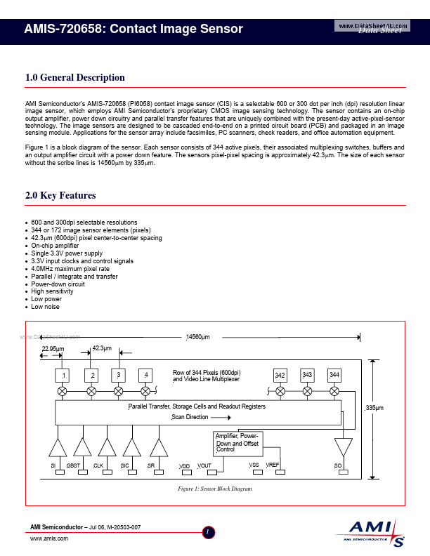
- The internal shift register starts the scan after GBST is clocked in on the falling edge of the clock input (CLK)
- A sequence of cascaded sensors has a unique first sensor and identically behaving subsequent sensors
- With its SIC tied high (Vdd), the first sensor self-starts the readout of its pixels after 82 clock cycles of delay
- With their SIC tied low (Ground), all of the subsequent sensors delay their readout of their pixels until after they receive a SI pulse
- Furthermore, the first sensor’s SI is left unconnected, while the subsequent