DESCRIPTION
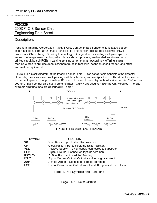
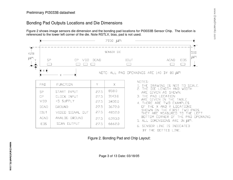
: Peripheral Imaging Corporation PI3033B CIS, Contact Image Sensor, chip is a 200 dot per inch resolution, linear array image sensor chip. Accordingly offering image reading widths to suit document scanners found in facsimile, scanner, check reader, and office automation equipment. Figure 1 is a block diagram of the imaging sensor chip. Each sensor chip consists of 64 detector elements, their associated multiplexing switches, buffers, and a chip selector. The detector's elementto-element spacing is approximately 125 um. The size of each chip without scribe lines is 7950 um by 500 um. Each sensor chip has 8 bonding pads. Only 7 are used to make the CIS Modules. The pad symbols and functions are described in Table 1. 7950 m Row of 64 Sensors and Video Signal Multiplexers Readout Shift Register 500 m Buffer SP Buffer CP VDD DGND Chip Select IOUT RSTLEV Buffer AGND EOS Figure 1. PI3033B Block Diagram SYMBOL SP CP VDD DGND RSTLEV IOUT AGND EOS FUNCTION Start Pulse: Input to start the line scan. AMI SEMICONDUCTOR