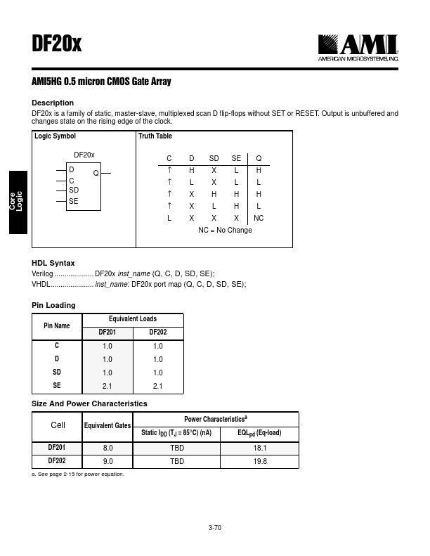
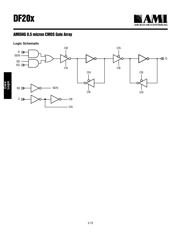
DESCRIPTION
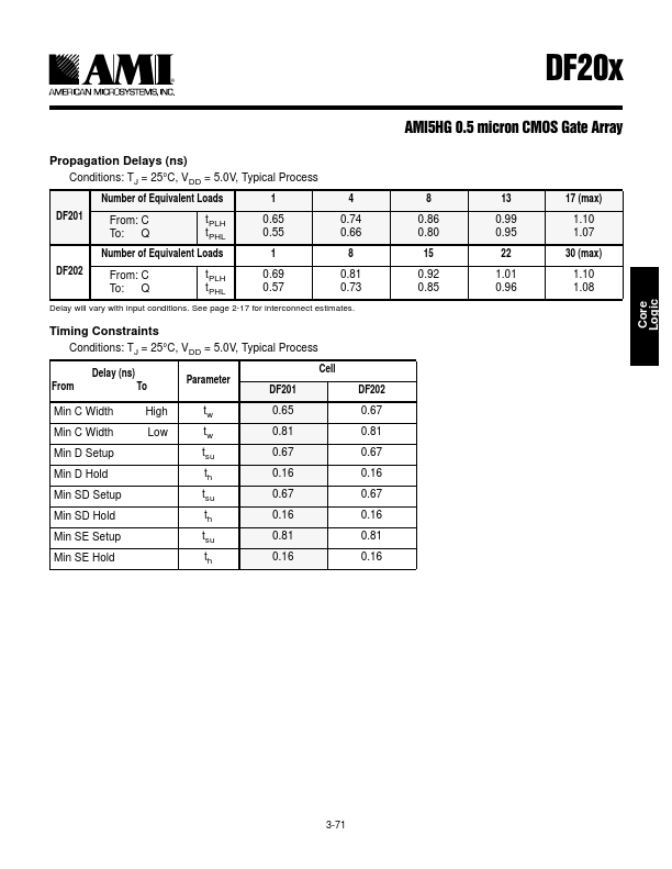
Output is unbuffered and changes state on the rising edge of the clock. Logic Symbol Truth Table DF20x DQ C SD SE C D SD SE Q ↑HX LH ↑LXLL ↑ XHHH ↑XLHL L X X X NC NC = No Change HDL Syntax Verilog .................... DF20x inst_name (Q, C, D, SD, SE); VHDL...................... inst_name: DF20x port map (Q, C, D, SD, SE); Pin Loading Pin Name C D SD SE Equivalent Loads DF201 DF202 1.0 1.0 1.0 1.0 1.0 1.0 2.1 2.1 Size And Power Characteristics Cell Equivalent Gates Power Characteristicsa Static IDD (TJ = 85°C) (nA) EQLpd (Eq-load) DF201 8.0 TBD 18.1 DF202 9.0 TBD 19.8 a. See page 2-15 for power equation. 3-70 Core Logic ') [ ® $0, +* PLFURQ &026 *DWH $UUD\ Propagation Delays (ns) Conditions: TJ = 25°C, VDD = 5.0V, Typical Process Number of Equivalent Loads 1 4 DF201 Fro AMI