ODTSXN12
ODTSXN12 is CMOS Gate Array manufactured by AMI.
- Part of the ODTSXN04 comparator family.
- Part of the ODTSXN04 comparator family.
2'76;1[[
®
$0,+- PLFURQ &026
- DWH $UUD
Description
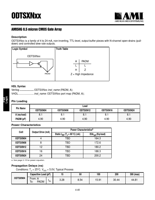
ODTSXNxx is a family of 4 to 24 mA, non-inverting, TTL-level, output buffer pieces with N-channel open-drains (pulldown) and controlled slew rate outputs.
Logic Symbol
Truth Table
ODTSXNxx
PADM
A PADM LL HZ Z = High Impedance
Pad Logic
HDL Syntax Verilog .................... ODTSXNxx inst_name (PADM, A); VHDL...................... inst_name: ODTSXNxx port map (PADM, A);
Pin Loading
Pin Name A (eq-load) PADM (pF)
ODTSXN04 8.1 4.90
ODTSXN08 8.1 4.90
Load ODTSXN12
8.1 4.90
ODTSXN16 8.1 4.90
ODTSXN24 8.1 4.90
Power Characteristics
Cell Output Drive (mA)
ODTSXN04
ODTSXN08
ODTSXN16
ODTSXN24...