ON11
ON11 is CMOS Gate Array manufactured by AMI.
21[
®
$0,+- PLFURQ &026
- DWH $UUD
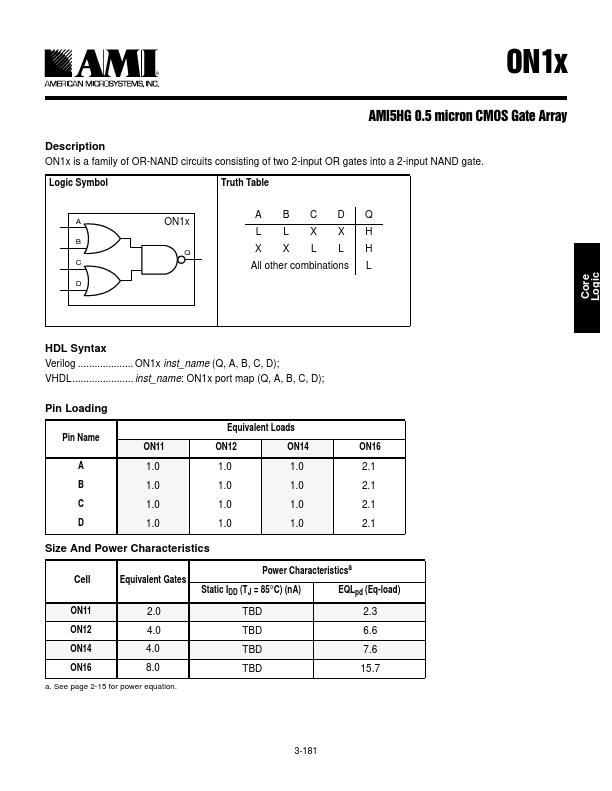
Description ON1x is a family of OR-NAND circuits consisting of two 2-input OR gates into a 2-input NAND gate.
Logic Symbol
Truth Table
ON1x
A B CDQ
L LXXH
Q XXL LH
C All other binations L
Core Logic
HDL Syntax Verilog .................... ON1x inst_name (Q, A, B, C, D); VHDL...................... inst_name: ON1x port map (Q, A, B, C, D);
Pin Loading
Pin Name
ON11 1.0 1.0 1.0 1.0
Equivalent Loads
ON12
ON14
1.0 1.0
1.0 1.0
1.0 1.0
1.0 1.0
ON16 2.1 2.1 2.1 2.1
Size And Power Characteristics
Power Characteristicsa
Cell Equivalent Gates
Static IDD (TJ = 85°C) (n A)
EQLpd...