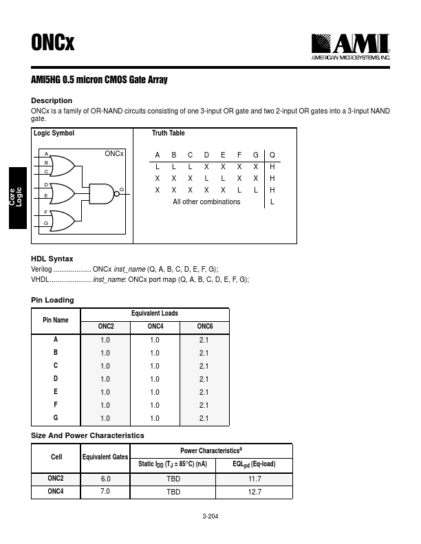
DESCRIPTION
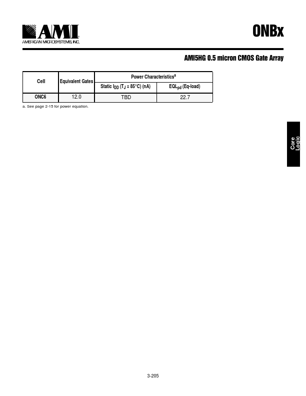
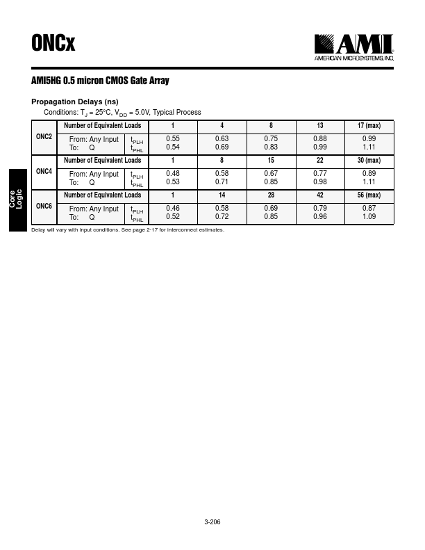
Logic Symbol Truth Table A ONCx A BCDE FGQ B L L LXXXXH C XXXL LXXH D Q XXXXXL LH E All other combinations L F G Core Logic HDL Syntax Verilog .................... ONCx inst_name (Q, A, B, C, D, E, F, G); VHDL...................... inst_name: ONCx port map (Q, A, B, C, D, E, F, G); Pin Loading Pin Name A B C D E F G ONC2 1.0 1.0 1.0 1.0 1.0 1.0 1.0 Equivalent Loads ONC4 1.0 1.0 1.0 1.0 1.0 1.0 1.0 ONC6 2.1 2.1 2.1 2.1 2.1 2.1 2.1 Size And Power Characteristics Power Characteristicsa Cell Equivalent Gates Static IDD (TJ = 85°C) (nA) EQLpd (Eq-load) ONC2 6.0 TBD 11.7 ONC4 7.0 TBD 12.7 3-204 21%[ ® $0, +* PLFURQ &026 *DWH $UUD\ Cell Equivalent Gates ONC6 12.0 a. See page 2-15 for power equation. Power Characteristicsa Static IDD (TJ = 85°C) (nA) EQLpd (Eq-load) TBD AMI