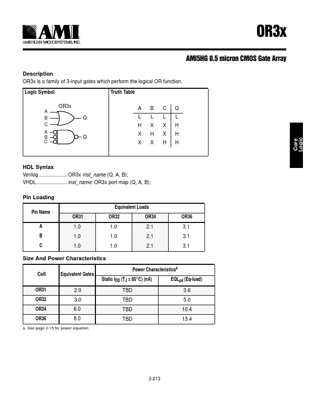
DESCRIPTION
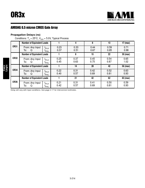
Logic Symbol Truth Table OR3x A BQ C A BQ C A B CQ LLLL HXXH XHXH XXHH HDL Syntax Verilog .................... OR3x inst_name (Q, A, B); VHDL...................... inst_name: OR3x port map (Q, A, B); Pin Loading Pin Name A B C OR31 1.0 1.0 1.0 Equivalent Loads OR32 OR34 1.0 2.1 1.0 2.1 1.0 2.1 OR36 3.1 3.1 3.1 Size And Power Characteristics Cell OR31 Equivalent Gates 2.0 Power Characteristicsa Static IDD (TJ = 85°C) (nA) EQLpd (Eq-load) TBD 3.6 OR32 OR34 OR36 3.0 6.0 8.0 TBD TBD TBD 5.0 10.4 13.4 a. See page 2-15 for power equation. 3-213 25 [ $0, +* PLFURQ &026 *DWH $UUD\ Propagation Delays (ns) Conditions: TJ = 25°C, VDD = 5.0V, Typical Process OR31 Number of Equivalent Loads From: Any Input To: Q tPLH tPHL Number of Equivalent Loads 1 0.23 0.37 1 4 0.33 0.51 8 OR32 From: Any Input To: Q tPLH tPHL AMI