FEATURES
Power supply - VDD: 3.3V VDDQ : 3.3V LVTTL compatible with multiplexed address Two banks / Pulse RAS MRS cycle with address key programs - CAS Latency (2 & 3) - Burst Length (1,2,4,8 & full page) - Burst Type (Sequential & Interleave) Clock Frequency (max) : 167MHz @ CL=3 (-6) 143MHz @ CL=3 (-7) 512K X 32 Bit X 2 Banks Synchronous DRAM All inputs are sampled at the positive going edge of the system clock DQM for masking Auto & self refresh 64ms refresh period (4K cycle) Industrial operating temperature range: -40ºC to +85ºC for -U series. Available in 90 Balls CSP (8mm X 13mm) Package is available to lead free (-F series) GENERAL DESCRIPTION
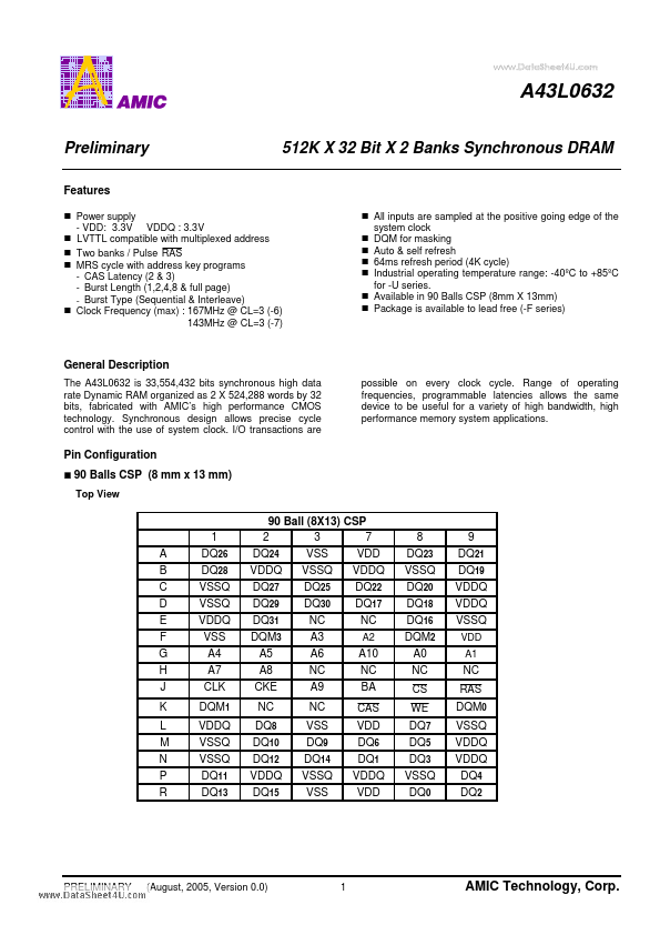
Synchronous design allows precise cycle control with the use of system clock. I/O transactions are possible on every clock cycle. Range of operating frequencies, programmable latencies allows the same device to be useful for a variety of high bandwidth, high performance memory system applications. Pin Configuration 90 Balls CSP (8 mm x 13... AMIC Technology