AM3929
AM3929 is manufactured by AMtek.
AM3929 Motor Driver ICs
Single Phase Full-Wave Motor Driver for Fan Motor AM3929
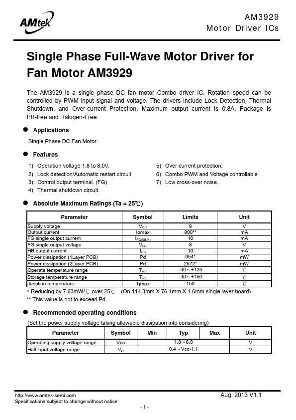
The AM3929 is a single phase DC fan motor bo driver IC. Rotation speed can be controlled by PWM input signal and voltage. The drivers include Lock Detection, Thermal Shutdown, and Over-current Protection. Maximum output current is 0.8A. Package is PB-free and Halogen-Free.
- Applications
Single Phase DC Fan Motor.
- Features
1) Operation voltage 1.8 to 8.0V. 2) Lock detection/Automatic restart circuit. 3) Control output terminal. (FG) 4) Thermal shutdown circuit.
5) Over current protection. 6) bo PWM and Voltage controllable 7) Low cross-over noise.
-...