Datasheet4U.com
🌙
AM3933 Datasheet | AMtek
Part:
AM3933
Description:
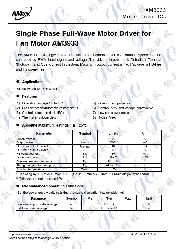
Single Phase Full-Wave Motor Driver
Manufacturer:
AMtek
Size:
439.00 KB
AM3933 Datasheet (PDF) Download
AMtek
AM3933
Key Features
1) Operation voltage 1.8 to 8.0V. 2) Lock detection/Automatic restart circuit. 3) Control output terminal. (FG) 4) Thermal shutdown circuit
×
Close