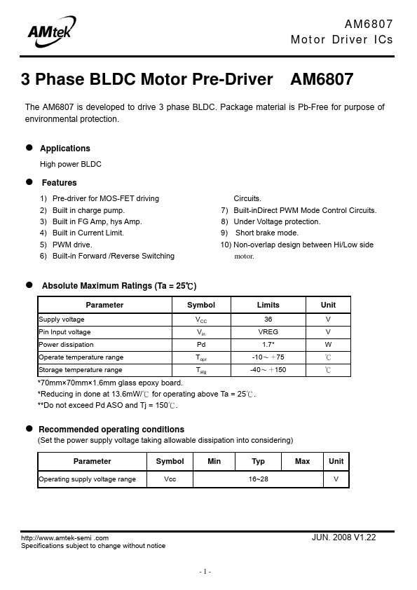
Description
PIN No
1
2 3 4 5 6 7 8 9 10 11 12 13 14 15 16 17
18
19 20 21 22 23 24 25 26 27 28
29
30 31 32 33 34
Pin Name
GND
CL UHG ULG VHG VLG WHG WLG D-PWM Vcc OSC Vb CP2 CP1 VREG HU+ HU-
HV+
HVHW+ HWFGin+ FGinFGout FGsout F/R DEC ACC
RCP
CPout Pref Rfe Cfe CNF
Function
GND pin
Current limit pin
FET gate p
Features
- 1) Pre-driver for MOS-FET driving 2) Built in charge pump. 3) Built in FG Amp, hys Amp. 4) Built in Current Limit. 5) PWM drive. 6) Built-in Forward /Reverse Switching
Circuits. 7) Built-inDirect PWM Mode Control Circuits. 8) Under Voltage protection. 9) Short brake mode. 10) Non-overlap design between Hi/Low side
motor. z Absolute Maximum Ratings (Ta = 25℃)
Parameter
Symbol
Limits
Supply voltage
VCC 36
Pin Input voltage
Vin VREG
Power dissipation
Pd 1.7.
- Operate temperature rang.