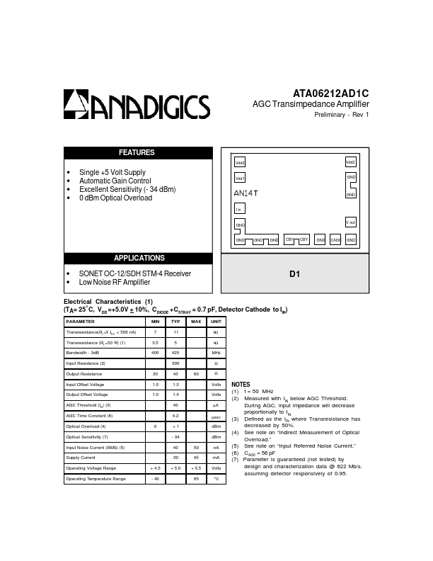
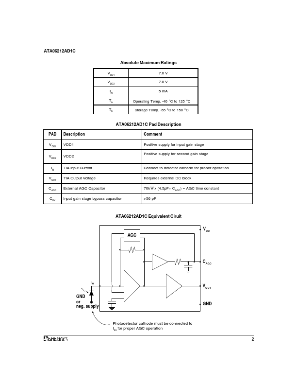
PAD V DD1 V DD2 IIN V OUT C AGC C BY Description VDD1 VDD2 TIA Input Current TIA Output Voltage External AGC Capacitor Input gain stage bypass capacitor Comment Positive supply for input gain stage Positive supply for second gain stage
Connect to detector cathode for proper operation Requires exter
Key Features
Vdd2 Vdd2.
Single +5 Volt Supply Automatic Gain Control Excellent Sensitivity (- 34 dBm) 0 dBm Optical Overload
Vdd1
GND
GND
I in
GND
V out
GND
GND
GND
CBY
CBY
GND
CAGC
GND.
Full PDF Text Transcription for ATA06212AD1C (Reference)
Note: Below is a high-fidelity text extraction (approx. 800 characters) for
ATA06212AD1C. For precise diagrams, and layout, please refer to the original PDF.
ATA06212AD1C AGC Transimpedance Amplifier Preliminary - Rev 1 FEATURES Vdd2 Vdd2 • • • • Single +5 Volt Supply Automatic Gain Control Excellent Sensitivity (- 34 dBm) 0 d...
View more extracted text
olt Supply Automatic Gain Control Excellent Sensitivity (- 34 dBm) 0 dBm Optical Overload Vdd1 GND GND I in GND V out GND GND GND CBY CBY GND CAGC GND APPLICATIONS • SONET OC-12/SDH STM-4 Receiver • Low Noise RF Amplifier Electrical Characteristics (1) (TA= 25°C, VDD =+5.0V + 10%, CDIODE +CSTRAY = 0.