ANADIGICS Inc ATA06212AD1C
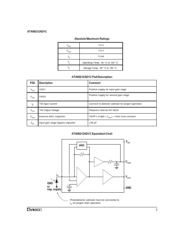
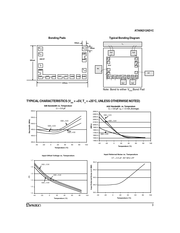
The ATA06212AD1C may be operated from a positive supply as low as + 4.5 V and as high as + 6.0 V. The power supply bypass capacitors should be mounted on or connected to a good low inductance ground plane.| Part No. | ATA06212AD1C |
|---|---|
| Datasheet | ATA06212AD1C Download |
| Manufacturer |  ANADIGICS Inc |
| Description | AGC TRANSIMPEDANCE AMPLIFIER |
| Buy | Stock & Price |
FEATURES
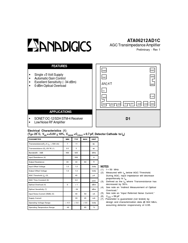
Vdd2 Vdd2●
●
●
● Single +5 Volt Supply Automatic Gain Control Excellent Sensitivity (- 34 dBm) 0 dBm Optical Overload Vdd1 GND GND I in GND V out GND GND GND CBY CBY GND CAGC GND
APPLICATIONS
● SONET OC-12/SDH STM-4 Receiver● Low Noise RF Amplifier
ELECTRICAL CHARACTERISTICS
(1) (TA= 25°C, VDD =+5.0V + 10%, CDIODE +CSTRAY = 0.7 pF, Detector Cathode to IIN) PARAMETER Transresistance(RL=¥ ,IDC < 500 nA) Transresistance (RL=50 W ) (1) Bandwidth - 3dB Input Resistance (2) Output Resistance Input Offset Voltage Output Offset Voltage AGC Threshold (IIN) (3) AGC Time Constant (6) Optical Overload (4) Optical Sensitivity (7) Input Noise Current (RMS) (5) Supply Current Operating Voltage Range Operating T emperature Range + 4.5 - 40 0 30 1.0 1.0 MIN 7 3.5 400 TYP 11 5 425 300 43 1.3 1.4 40 4.2 +1 - 34 40 30 + 5.0 50 45 + 5.5 85 60 MAX UNIT k Ω k Ω D1 MHz Ω Ω Volts Volts µA µsec dBm dBm nA mA Volts ° C NOTES (1) f = 50 MHz (2) Measured with IIN below AGC Threshold. During AGC, input i...