ALT6701
ALT6701 is Multimode PAM manufactured by ANADIGICS.
FEATURES
- CDMA/EVDO, WCDMA/HSPA and LTE pliant
- 4th Generation HELPTM technology
- High Efficiency (R99 waveform):
- 41 % @ POUT = +28.4 d Bm
- 31 % @ POUT = +17 d Bm
- 21 % @ POUT = +13.5 d Bm
- 26 % @ POUT = +9 d Bm
- 13 % @ POUT = +3.5 d Bm
- Low Quiescent Current: 2 m A
- Low Leakage Current in Shutdown Mode: <5 µA
- Internal Voltage Regulator
- Integrated “daisy chainable” directional coupler with CPLIN and CPLOUT port.
- Internal DC blocks on IN/OUT RF ports
- Optimized for a 50 Ω System
- 1.8 V Control Logic
- Ro HS pliant Package, 260 o C MSL-3
APPLICATIONS
- Band 1 WCDMA/HSPA Wireless Devices
- Band 1 LTE Wireless Devices
- Band Class 6 CDMA/EVDO Wireless Devices
PRODUCT DESCRIPTION
The ALT6701 HELP4TM PA is a 4th generation HELPTM product for LTE and WCDMA devices operating in UMTS2100 (Band 1) and for CDMA devices operating in Band Class 6. This PA incorporates ANADIGICS’ HELP4TM technology to deliver exceptional efficiency at low power levels and low quiescent current without the need for external voltage regulators or converters. The device is manufactured using advanced In Ga PPlus TM HBT technology offering state-of-the-art reliability, temperature stability, and ruggedness. Three selectable bias modes that optimize efficiency for different output power levels and a shutdown mode with low leakage current increase handset
HELP4TM UMTS2100 (Band 1) LTE, WCDMA, CDMA Multimode PAM
DATA SHEET
- Rev 2.8
M45 Package 10 Pin 3 mm x 3 mm x 1 mm
Surface Mount Module talk and standby time. A “daisy chainable” directional coupler is integrated in the module, thus eliminating the need of an external coupler. The self-contained 3 mm x 3 mm x 1 mm surface mount package incorporates matching networks optimized for output power, efficiency, and linearity in a 50 Ω system.
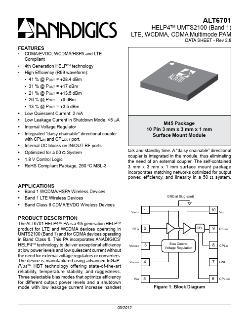
VBATT 11
GND at Slug (pad)
1100 VCC
RFIN 22
9 RFOUT
33VMODE2 44VMODE1
Bias Control Voltage Regulation
88 CPLIN 77 GND
VEN 55
Figure 1: Block...