APS3628
APS3628 is Active Splitters manufactured by ANADIGICS.
aDVANCED PRODUCT INFORMATION
- Rev 0.1
Eight-way Active Power Splitter
- Single Input, Eight Output Design
- Wideband Operation to above 1 GHz
- Nominal 3.2 dB Gain
- 4.7 dB Typical Noise Figure
- Single +3.3V or +5V Supply
- High Linearity, Low Distortion
- Current adjust pin for optimizing distortion performance
- Single-Ended 75 Ohm Inputs/Outputs
- Materials set consistent with RoHS Directives
Features
APPLICATIONS
- All-Digital CATV Set-Top Boxes with Multiple Tuners
- Home Gateways, Multiple-Tuner TVs and Set-top boxes
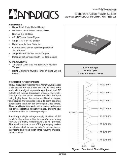
S34 Package 24 Pin QFN 4 mm x 4 mm x 1 mm
This APS3628 active splitter from ANADIGICS accepts a broadband RF input from 50...