AWS5518 Overview
Description
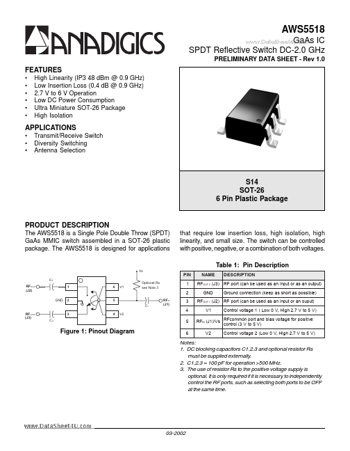
RFOUT 2 (J3) RF port (can be used as an input or as an output) GND Ground connection (keep as short as possible) 2 5 C1 RFIN (J1) 3 4 5 RFOUT 1 (J2) RF port (can be used as an input or an ouput) V1 Control voltage 1 ( Low 0 V, High 2.7 V to 5 V) RF OUT2 (J3) 3 C2 4 V2 RFcommon port and bias voltage for positive RFIN (J1)/Vs control (3 V to 5 V) V2 Control voltage 2 (Low 0 V, High 2.7 V to 5 V) Figure 1: Pinout Diagram 6 Notes: 1. DC blocking capacitors C1,2,3 and optional resistor Rs must be supplied externally.