FEATURES
High Output Intercept Point High Linearity True Surface Mount Package Internal Bias Circuit Requiring Nominal Input Voltages + 10% Low Cost Off Chip Output Matching Circuit Allows Application Optimization AWT1921 PRELIMINARY DATA SHEET - Rev 1.0 PRODUCT DESCRIPTION
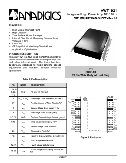
Table 1: Pin DESCRIPTION
PIN 1,14,15,28, slug 2 27 4 3 5,6,7,8 9,10 11 26 12 13 16,17 18-25 N AME GND VGS1 & RFIN V DD V D2 V D1 GND V D3 VGS2 VREF V SS VGS3 VGS4 V D4 D ESC R IPTION AC and RF Ground Fi rst Stage Gate termi nal & RF Input Posi ti ve Supply of Bi as C i rcui t(+5V) Second Stage drai n supply (+9V Fi rst Stage drai n supply (+9V) Fi rst and Second Stage Source ground Thi rd Stage drai n supply (+9V) Second Stage Gate Termi nal Bi as control Pi n (+5V) Negati ve Supply for Bi as C i rcui t (-5V) Thi rd Stage Gate termi nal Fourth Stage Gate termi nal Fourth Stage drai n supply (+9V) & RF out S11 SSOP-28 28 Pin Wide Body w/ Heat Slug Pin 1 GND VGS1/RFIN VD1 VD2 GND GND GND GND VD3 VD3 VGS2 V... ANADIGICS