FEATURES
PRELIMINARY DATA SHEET - Rev 1.0 InGaP HBT Technology Integrated Power Control (CMOS) Quad Band APPLICATIONS
+35 dBm GSM Output Power at 3.5 V +33 dBm DCS/PCS Output Power at 3.5 V 55% GSM PAE 50% DCS/PCS PAE Small Footprint: 7 x 10mm Low Profile: 1.4mm Power Control Range: >50 dB GPRS Capable (Class 12) Moisture Sensitivity Level (MSL) 3 at 260 °C AWT6108 AW T 610 8 APPLICATIONS
GSM850/GSM900/DCS/PCS Handsets 20 Pin 7mm x 10mm Surface Mount Module Dual/Tri/Quad Band PDA PRODUCT DESCRIPTION
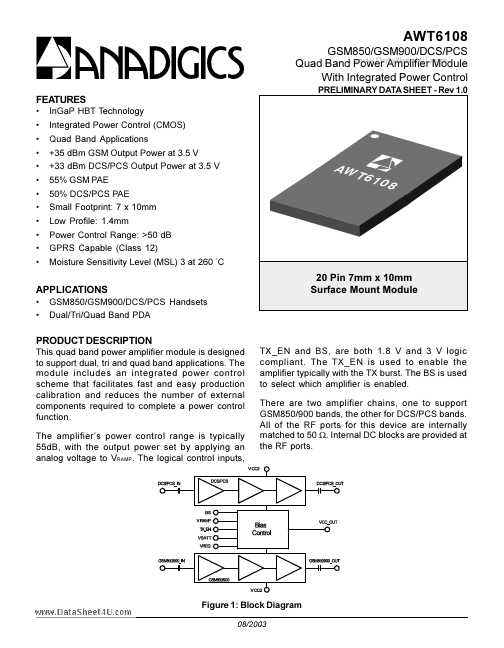
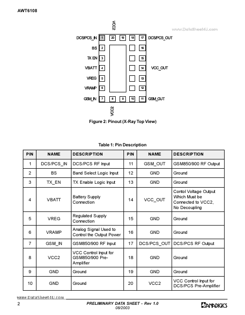
The amplifiers power control range is typically 55dB, with the output power set by applying an analog voltage to VRAMP. The logical control inputs, TX_EN and BS, are both 1.8 V and 3 V logic compliant. The TX_EN is used to enable the amplifier typically with the TX burst. The BS is used to select which amplifier is enabled. There are two amplifier chains, one to support GSM850/900 bands, the other for DCS/PCS bands. All of the RF ports for this device are internally matched to 50 W. ANADIGICS