GENERAL DESCRIPTION
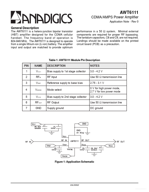
The frequency band of operation is 824-849 MHz. The amplifier input and output are matched to provide optimum performance in a 50 Ω system. Minimal external components are required for proper RF bypassing. The tantalum capacitors, C8 and C9, are not required. Landings should be made available on the printed circuit board (PCB) as a precaution. Table 1: AWT6111 Module Pin DESCRIPTION
PIN 1 2 3 4 5 6 7 NAME V CC1 RFIN VREF VMODE V CC2 RFOUT GND DESCRIPTION
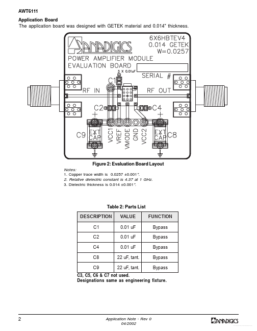
Bias supply to 1st stage collector RF Input Reference supply to base bias Mode select Bias supply to 2nd stage collector RF Output Supply ground NOTES 3.0 - 4.2 V Use 50 Ω transmission line 2.75 - 3.1 V 0 V for high power mode, 2.7 V for low power mode 3.0 - 4.2 V Use 50 Ω transmission line DC ground Figure 1: Application Schematic 04/2002 Free Datasheet AWT6111 Application Board The application board was designed with GETEK material and 0.014" thickness. Figure 2: Evaluation Board Layout Notes: 1. Copper trace width is 0.0257 ±0.001". ANADIGICS