ANADIGICS AWT921
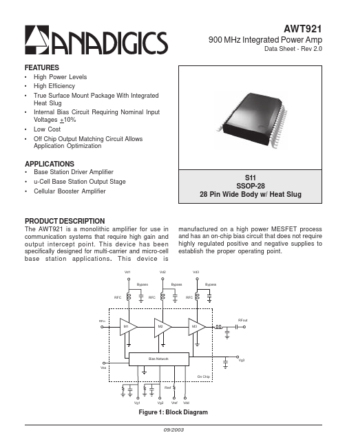
The AWT921 is a monolithic amplifier for use in communication systems that require high gain and output intercept point. This device has been specifically designed for multi-carrier and micro-cell base station applications . This device is Vd1 Vd2 manufactured on a high power MESFET process and has an on-chip bias circuit that does not require highly regulated positive and negative supplies to establish the proper operating point.| Part No. | AWT921 |
|---|---|
| Datasheet | AWT921 Download |
| Manufacturer |  ANADIGICS |
| Description | 900MHz Integrated Power Amp |
| Buy | Stock & Price |
FEATURES
●●
●
●
●
● High Power Levels High Efficiency True Surface Mount Package With Integrated Heat Slug Internal Bias Circuit Requiring Nominal Input Voltages +10% Low Cost Off Chip Output Matching Circuit Allows Application Optimization
APPLICATIONS
●●
● Base Station Driver Amplifier u-Cell Base Station Output Stage Cellular Booster Amplifier S11 SSOP-28 28 Pin Wide Body w/ Heat Slug PRODUCT
DESCRIPTION
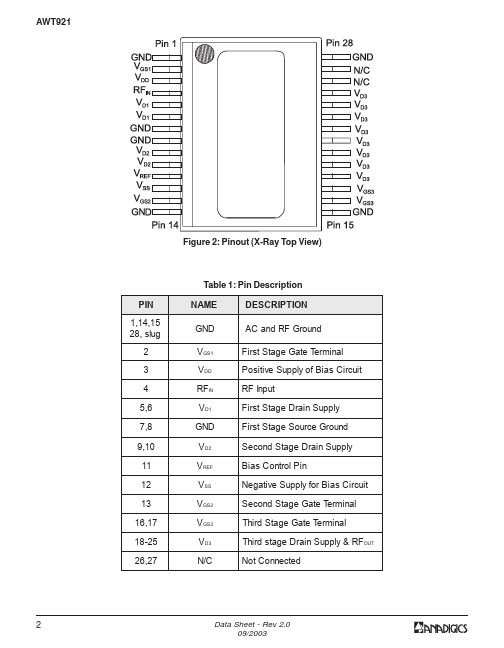
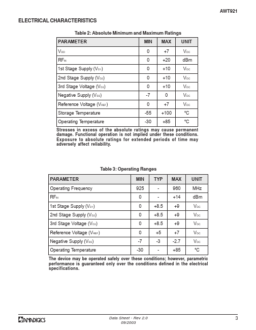
Vd3 Bypass Bypass Bypass RFC RFC RFC RFin RFout M1 M2 M3 Bias Network Vss On Chip Rref Vg3 Vg1 Vg2 Vref Vdd Figure 1: Block Diagram 09/2003 AWT921 Figure 2: Pinout (X-Ray Top View) Table 1: PinDESCRIPTION
PIN 1,14,15 28, slug 2 3 4 5,6 7,8 9,10 11 12 13 16,17 18-25 26,27 NAME GND VGS1 V DD RFIN V D1 GND V D2 VREF V SS VGS2 VGS3 V D3 N/CDESCRIPTION
AC and RF Ground First Stage Gate Terminal Positive Supply of Bias Circuit RF Input First Stage Drain Supply First Stage Source Ground Second Stage Drain Supply Bias Control Pin Negative Supply for Bias Circuit Second Stage Gate Termin...