AP358 Overview
Description
OP-Amp1 Output OP-Amp1’s Inverting Input OP-Amp1’s Non-inverting Input GND OP-Amp2’s Non-inverting Input OP-Amp2’s Inverting Input OP-Amp2 Output Vcc for Dual Operational Amplifier REV. 00 2 AP358 Parameter Supply Voltage Differential input voltage Input voltage Power Dissipation Operating temperature Storage temperature Symbol VCC VIND VIN PD TOPR TSTG Values 36 or ±18 32 -0.3 ~ +32 600 -45 ~ +85 -55 ~ +150 Units V V V mW ℃ ℃ Characteristics Input offset voltage Input offset voltage drift Input offset current Symbol VIOS ΔVIOS/ΔT IIOS Test Condition 5V≤VCC≤30V (Ta = 25℃) Rg = 0Ω, 0V≤VIC≤VCC-1.5V Rg = 0Ω - (Ta = 25℃) Input offset current drift Input bias current ΔIIOS/ΔT IIB - (Ta = 25℃) Input common mode voltage range Supply current Large signal voltage gain Output voltage swing Common mode rejection ratio Power supply rejection ratio Output source current Output sink current Output short circuit to ground VICR ICC GV VOH VOL CMRR VCC = 30V (Ta = 25℃) VCC = 30V, RL = ∞ VCC = 5V, RL.
Key Features
- Input common mode voltage range includes ground
- Internally frequency compensated for unity gain
- Large DC voltage gain : 100dB
- Wide Bandwidth for unity gain : 1 MHz
- Very low power consumption
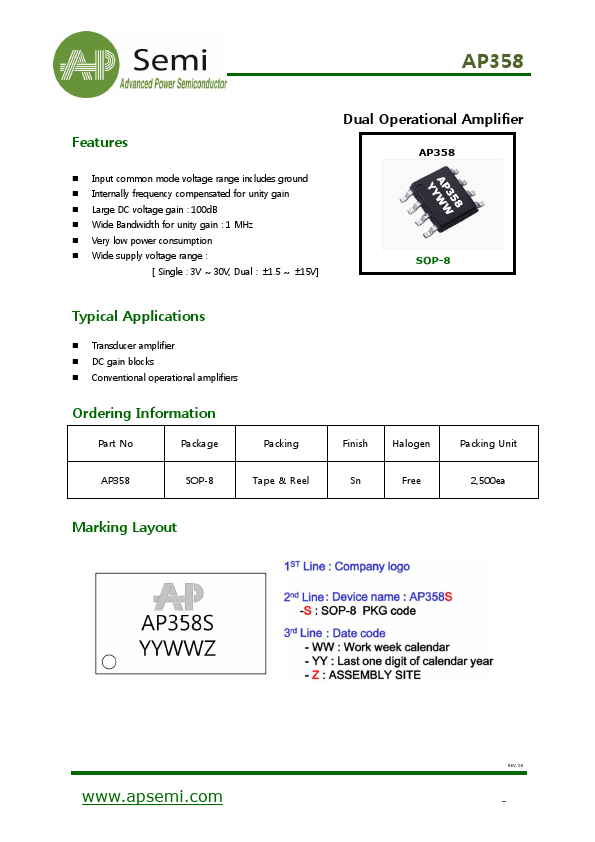
- Wide supply voltage range : [ Single : 3V ~ 30V, Dual : ±1.5 ~ ±15V] Dual Operational Amplifier AP358 SOP-8