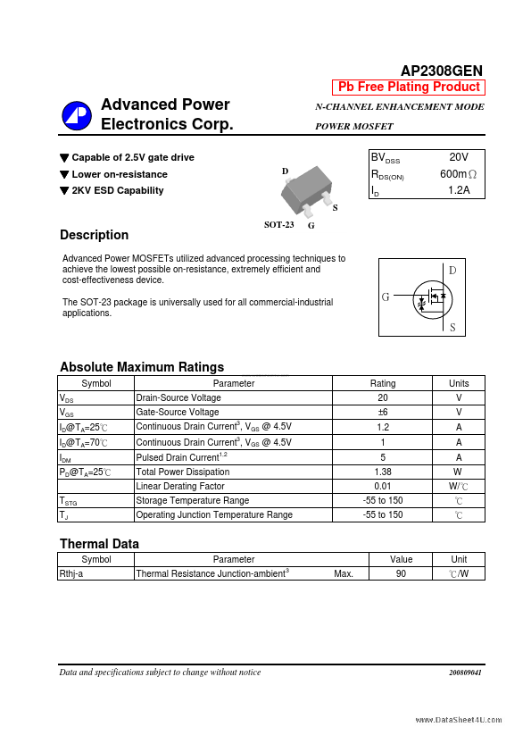
DESCRIPTION
Advanced Power MOSFETs utilized advanced processing techniques to achieve the lowest possible on-resistance, extremely efficient and cost-effectiveness device. D G S ABSOLUTE MAXIMUM RATINGS
Symbol VDS VGS ID@TA=25℃ ID@TA=70℃ IDM PD@TA=25℃ TSTG TJ Drain-Source Voltage Gate-Source Voltage Parameter Rating 20 ±6 Units V V A A A W W/ ℃ ℃ ℃ Continuous Drain Current , VGS @ 4.5V Continuous Drain Current , VGS @ 4.5V Pulsed Drain Current 1,2 3 3 1.2 1 5 1.38 0.01 -55 to 150 -55 to 150 Total Power Dissipation Linear Derating Factor Storage Temperature Range Operating Junction Temperature Range Thermal Data Symbol Rthj-a Parameter Thermal Resistance Junction-ambient 3 Value Max. 90 Unit ℃/W Data and specifications subject to change without notice 200809041 AP2308GEN ELECTRICAL CHARACTERISTICS
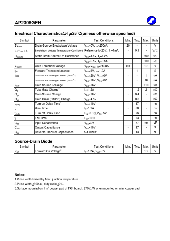
@Tj=25oC(unless otherwise specified) Symbol BVDSS ΔBVDSS/ΔTj Parameter Drain-Source Breakdown Voltage Test Conditions VGS=0V, ID=250uA Min. 20 0.5 - Typ. 0.1 1 1.2 0.4 0.3 17 36 76 73 37 17 13 Max. Advanced Power Electronics