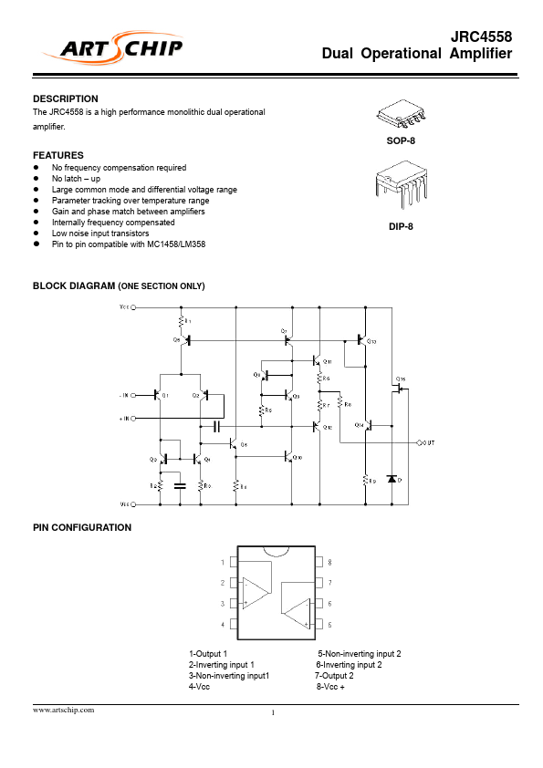
DESCRIPTION
FEATURES
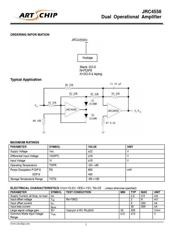
z No frequency compensation required z No latch – up z Large common mode and differential voltage range z Parameter tracking over temperature range z Gain and phase match between amplifiers z Internally frequency compensated z Low noise input transistors z Pin to pin compatible with MC1458/LM358 BLOCK DIAGRAM (ONE SECTION ONLY) JRC4558 Dual Operational Amplifier SOP-8 DIP-8 PIN CONFIGURATION 1-Output 1 2-Inverting input 1 3-Non-inverting input1 4-Vcc 1 5-Non-inverting input 2 6-Inverting input 2 7-Output 2 8-Vcc + ORDERING INFOR MATION Typical Application JRC4558 Dual Operational Amplifier MAXIMUM RATINGS
PARAMETER Supply Voltage Differential Input Voltage Input Voltage Operating Temperature Power Dissipation P-DIP 8 SOP 8 Storage Temperature Range SYMBOL Vcc VI(DIFF) VI TOPR PD TSTG VALUE ±22 ±18 ±15 -20~ +85 600 400 -65~+150 UNIT V V V mW ELECTRICAL CHARACTERISTICS
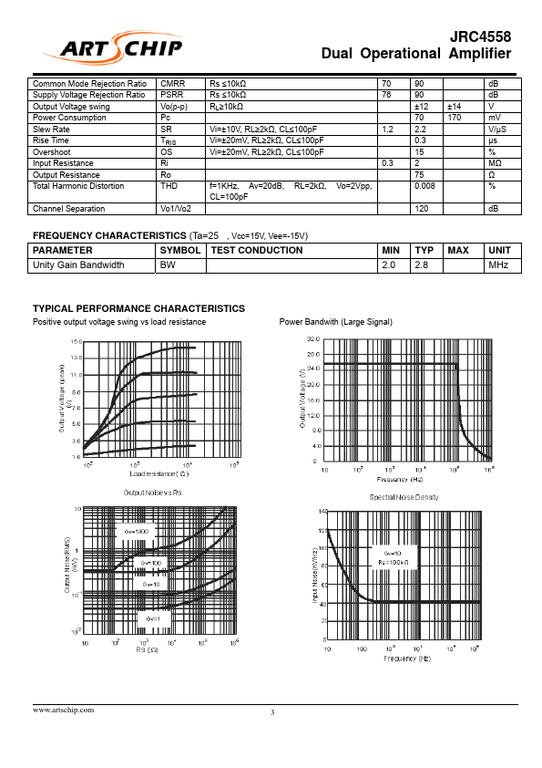
(Vcc=15.0V, VEE=-15V, TA=25 PARAMETER Supply Current, all Amp, no load Input offset voltage Input o... ART CHIP