FEATURES
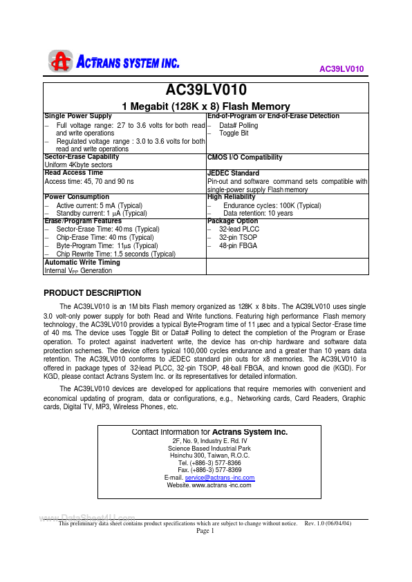
− Sector-Erase Time: 40 ms (Typical) − Chip-Erase Time: 40 ms (Typical) − Byte-Program Time: 11µs (Typical) − Chip Rewrite Time: 1.5 seconds (Typical) Automatic Write Timing Internal VPP Generation End-of-Program or End-of-Erase Detection − Data# Polling − Toggle Bit CMOS I/O Compatibility JEDEC Standard Pin-out and software command sets compatible with single-power supply Flash memory High Reliability − Endurance cycles: 100K (Typical) − Data retention: 10 years Package Option − 32-lead PLCC − 32-pin TSOP − 48-pin FBGA PRODUCT DESCRIPTION
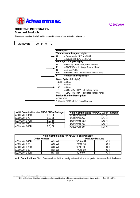
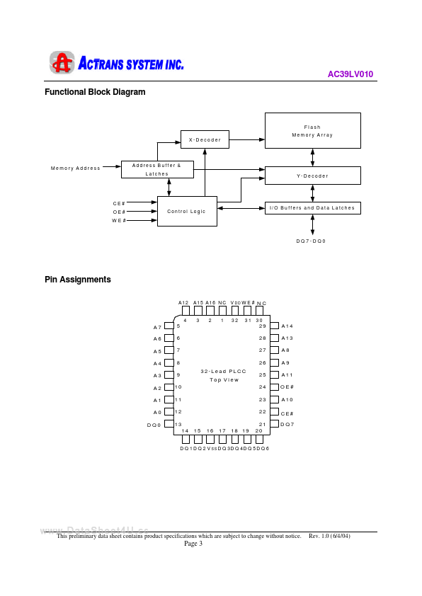
The device uses Toggle Bit or Data# Polling to detect the completion of the Program or Erase operation. To protect against inadvertent write, the device has on-chip hardware and software data protection schemes. The device offers typical 100,000 cycles endurance and a great er than 10 years data retention. The AC39LV010 conforms to JEDEC standard pin outs for x8 memories. The AC39LV010 is offered in package types of 32-lead PLCC, 32 -pin TSOP, 48-ball FBGA, and known good die (KGD). AS