AS4LC4M4883C
AS4LC4M4883C is EDO PAGE MODE manufactured by ASI.
FEATURES
- Industry-standard x4 pinout, timing, functions and packages
- High-performance CMOS silicon-gate process
- Single +3.3V ± 0.3V power supply
- Low power, 1m W standby; 150m W active, typical
- All inputs, outputs and clocks are TTL-patible
- Refresh modes: ?R?A/S ONLY, ?C?A/S-BEFORE-?R?A/S (CBR) HIDDEN
- 2,048-cycle (11 row-, 11 column-addresses)
- Extended Data-Out (EDO) PAGE access cycle
- 5V-tolerant I/Os (5.5V maximum VIH level)
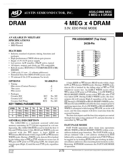
VCC DQ1 DQ2 /W/E /R/A/S NC A10 A0 A1 A2 A3 VCC
OPTIONS
- Timing 60ns access (Contact Factory) 70ns acess 80ns access
- Packages Ceramic SOJ Ceramic LCC Ceramic Gull Wing
MARKING
-6 -7 -8 ECJ EC ECG No. 505 No. 212 No. 603
KEY TIMING PARAMETERS
SPEED -6 -7 -8 t RC 110ns 130ns 150ns t RAC 60ns 70ns 80ns t PC 30ns 35ns 40ns t AA 30ns 35ns 40ns t CAC 15ns 18ns 20ns t CAS 12ns 15ns 20ns
GENERAL DESCRIPTION
The AS4LC4M4 is a randomly accessed solid-state memory containing 16,777,216 bits organized in a x4 configuration. The AS4LC4M4 ?R?A/S is used to latch the first 11 bits and ?C?A/S the latter 11 bits. READ and WRITE cycles are selected with the ? W / E input. A logic HIGH on ?W/E dictates READ mode while a logic LOW on ?W/E dictates WRITE mode. During a WRITE cycle, data-in (D) is latched by the falling edge of ?W/E or ?C?A/S, whichever occurs last. If ?W/E goes LOW prior to ?C?A/S going LOW, the output pins remain open (High- Z) until the next ?C?A/S cycle, regardless of ?O/E.
AS4LC4M4 Rev. 11/97 DS000022
A logic HIGH on ?W/E dictates READ mode while a logic LOW on ?W/E dictates WRITE mode. During a WRITE cycle, data-in (D) is latched by the falling edge of ?W/E or /C/A/S, whichever occurs last. An EARLY WRITE occurs when ?W/E is taken LOW prior to /C/A/S falling. A LATE WRITE or READ-MODIFY-WRITE occurs when ?W/E falls after /C/A/S was taken LOW. During EARLY WRITE cycles, the dataoutputs (Q) will remain High-Z regardless of the state of O ? E / . During LATE WRITE or READ-MODIFY-WRITE cycles, ?O/E must be taken HIGH to disable...