ASI HVV1214-025
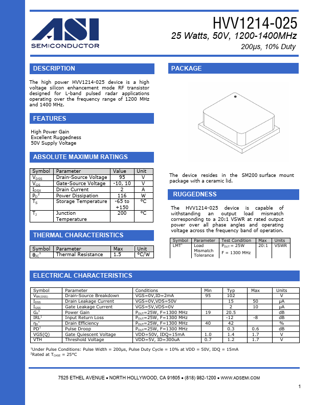
The HVV1214-025 device is capable of withstanding an output load mismatch corresponding to a 20:1 VSWR at rated output power over all phase angles and operating voltage across the frequency band of operation. This document supersedes and replaces all information supplied prior to the publication hereof.| Part No. | HVV1214-025 |
|---|---|
| Datasheet | HVV1214-025 Download |
| Manufacturer |  ASI |
| Description | RF transistor |
| Buy | Stock & Price |
DESCRIPTION
The high power HVV1214-025 device is a high voltage silicon enhancement mode RF transistor designed for L-band pulsed radar applications operating over the frequency range of 1200 MHz and 1400 MHz.FEATURES
High Power Gain Excellent Ruggedness 50V Supply VoltageABSOLUTE MAXIMUM RATINGS
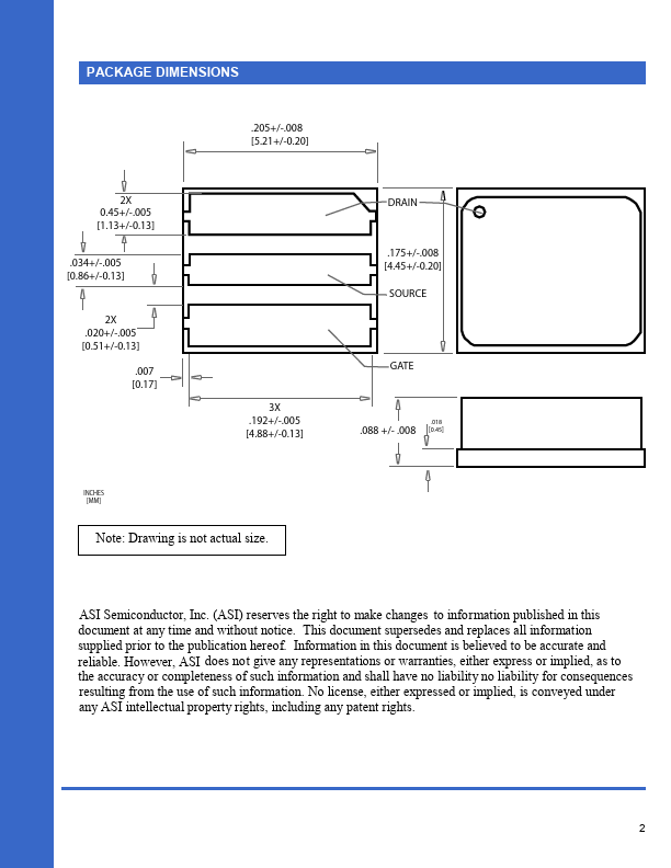
Symbol VDSS VGS IDSX PD2 TS TJ Parameter Drain-Source Voltage Gate-Source Voltage Drain Current Power Dissipation Storage Temperature Junction Temperature Value 95 -10, 10 2 116 -65 to +150 200 Unit V V A W °C °C THERMAL CHARACTERISTICS Symbol Parameter 1 JC Thermal Resistance Max 1.5 Unit °C/W PACKAGE The device resides in the SM200 surface mount package with a ceramic lid. RUGGEDNESS Symbol LMT1 Parameter Load Mismatch Tolerance Test Condition POUT = 25W F = 1300 MHz Max 20:1 Units VSWRELECTRICAL CHARACTERISTICS
Symbol VBR(DSS) IDSS IGSS GP1 IRL1 džD1 PD1 VGS(Q) VTH Parameter Drain-Source Breakdown Drain Leakage Current Gate Leakage Current Power Gain Input Return Loss Drain Efficiency Pul...