FEATURES
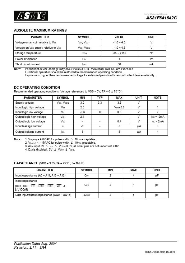
JEDEC standard 3.3V power supply LVTTL compatible with multiplexed address Four banks operation MRS cycle with address key programs - CAS Latency (2 & 3) - Burst Length (1, 2, 4, 8 & full page) - Burst Type (Sequential & Interleave) All inputs are sampled at the positive going edge of the system clock DQM for masking Auto & self refresh 15.6 µ s refresh interval 1M x 16 Bit x 4 Banks SYNCHRONOUS DYNAMIC RAM ORDERING INFORMATION 54 Pin TSOP (Type II) (400mil x 875mil ) PRODUCT NO. AS81F641642C-6 AS81F641642C-7 MAX FREQ. 166MHz 143MHz PACKAGE TSOP II AS81F641642C-6P AS81F641642C-7P 166MHz 143MHz TSOP II PB FREE GENERAL DESCRIPTION
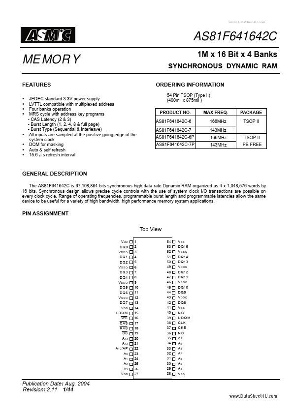
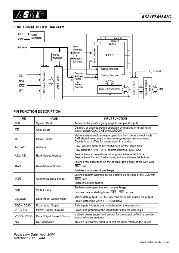
Synchronous design allows precise cycle controls with the use of system clock I/O transactions are possible on every clock cycle. Range of operating frequencies, programmable burst length and programmable latencies allow the same device to be useful for a variety of high bandwidth, high performance memory system applications. PIN ASSIGNMENT Top View V...