AP04200K
Features
- Advanced high cell density Trench technology
- Super Low Gate Charge
- Excellent Cd V/dt effect decline
- Green Device Available
40V P-Channel MOSFET
Product Summary
VDS ID RDS(ON)(at VGS=-10V) RDS(ON)(at VGS=-4.5V)
-40
-20
38 mΩ
55 mΩ
Applications
- High Frequency Point-of-Load,Synchronous Buck Converter
- Networking DC-DC Power System
- Load Switch
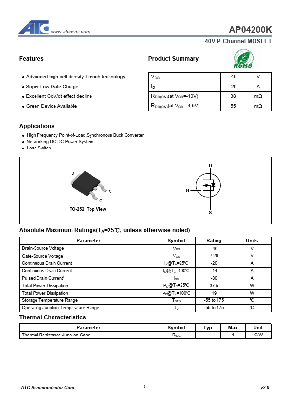
TO-252 Top View
Absolute Maximum Ratings(TA=25℃, unless otherwise noted)
Parameter Drain-Source Voltage Gate-Source Voltage Continuous Drain Current Continuous Drain Current Pulsed Drain Current2 Total Power Dissipation Total Power Dissipation Storage Temperature Range Operating Junction Temperature Range
Symbol VDS VGS
ID@TC=25℃ ID@TC=100℃
IDM PD@TC=25℃ PD@TC=100℃
TSTG TJ
Thermal Characteristics
Parameter Thermal Resistance Junction-Case1
Symbol RθJC
Rating -40 ±20 -20 -14 -80 37.5 19
-55 to 175 -55 to 175
Units V V A A A W W ℃ ℃
Typ
Max
Unit
---
℃/W
ATC Semiconductor...