ATC Semiconductor AT06700L
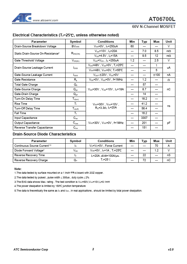
The data tested by surface mounted on a 1 inch2 FR-4 board with 2OZ copper. The test condition is VDD=50V,VGS=10V,L=0.1mH 4.The power dissipation is limited by 150℃ junction temperature 5.The data is theoretically the same as ID and IDM , in real applications , should be limited by total power dissipation.| Part No. | AT06700L |
|---|---|
| Datasheet | AT06700L Download |
| Manufacturer |  ATC Semiconductor |
| Description | 60V N-Channel MOSFET |
| Buy | Stock & Price |
FEATURES
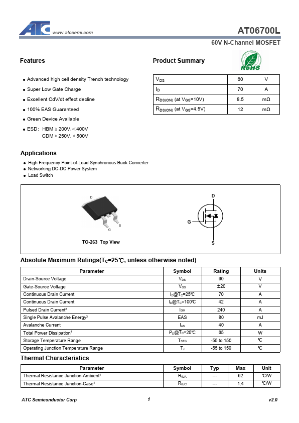
Product Summary● Advanced high cell density Trench technology
● Super Low Gate Charge
● Excellent CdV/dt effect decline
● 100% EAS Guaranteed
● Green Device Available
● ESD:HBM ≥ 200V,<400V CDM>250V,<500V VDS ID RDS(ON) (at VGS=10V) RDS(ON) (at VGS=4.5V) 60 V 70 A 8.5 mΩ 12 mΩ
APPLICATIONS
● High Frequency Point-of-Load Synchronous Buck Converter● Networking DC-DC Power System
● Load Switch D D G S G TO-263 Top View
ABSOLUTE MAXIMUM RATINGS
(TC=25℃, unless otherwise noted) Parameter Drain-Source Voltage Gate-Source Voltage Continuous Drain Current Continuous Drain Current Pulsed Drain Current2 Single Pulse Avalanche Energy3 Avalanche Current Total Power Dissipation4 Storage Temperature Range Operating Junction Temperature Range Symbol VDS VGS ID@TC=25℃ ID@TC=100℃ IDM EAS IAS PD@TC=25℃ TSTG TJ Thermal Characteristics Parameter Thermal Resistance Junction-Ambient1 Thermal Resistance Junction-Case1 Symbol RθJA RθJC ATC Semiconductor Corp 1 S Rating 60 ±20 70 42 240 80 40 65 -55...