ATC Semiconductor AT1045K
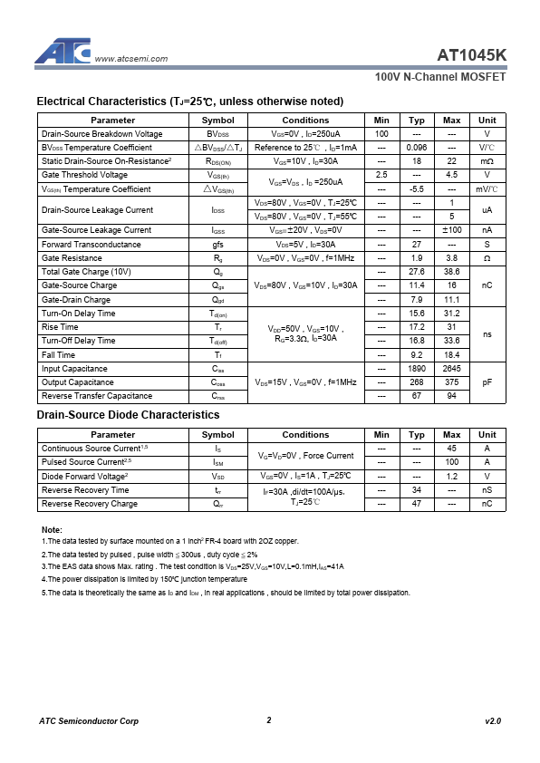
The data tested by surface mounted on a 1 inch2 FR-4 board with 2OZ copper. The test condition is VDS=25V,VGS=10V,L=0.1mH,IAS=41A 4.The power dissipation is limited by 150℃ junction temperature 5.The data is theoretically the same as ID and IDM , in real applications , should be limited by total power dissipation.| Part No. | AT1045K |
|---|---|
| Datasheet | AT1045K Download |
| Manufacturer |  ATC Semiconductor |
| Description | 100V N-Channel MOSFET |
| Buy | Stock & Price |
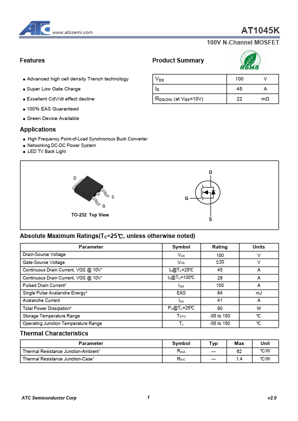
FEATURES
Product Summary● Advanced high cell density Trench technology
● Super Low Gate Charge
● Excellent CdV/dt effect decline
● 100% EAS Guaranteed
● Green Device Available
APPLICATIONS
● High Frequency Point-of-Load Synchronous Buck Converter● Networking DC-DC Power System
● LED TV Back Light VDS ID RDS(ON) (at VGS=10V) 100 V 45 A 22 mΩ D D S G G TO-252 Top View
ABSOLUTE MAXIMUM RATINGS
(TC=25℃, unless otherwise noted) Parameter Drain-Source Voltage Gate-Source Voltage Continuous Drain Current, VGS @ 10V1 Continuous Drain Current, VGS @ 10V1 Pulsed Drain Current2 Single Pulse Avalanche Energy3 Avalanche Current Total Power Dissipation4 Storage Temperature Range Operating Junction Temperature Range Symbol VDS VGS ID@TC=25℃ ID@TC=100℃ IDM EAS IAS PD@TC=25℃ TSTG TJ Thermal Characteristics Parameter Thermal Resistance Junction-Ambient1 Thermal Resistance Junction-Case1 Symbol RθJA RθJC S Rating 100 ±20 45 28 100 84 41 90 -55 to 150 -55 to 150 Units V V A A A mJ A W ℃ ℃ Typ Max Unit --...