25F512
Overview
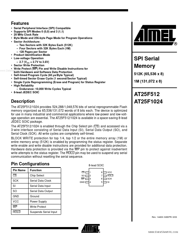
The AT25F512/1024 provides 524,288/1,048,576 bits of serial reprogrammable Flash memory organized as 65,536/131,072 words of 8 bits each. The device is optimized for use in many industrial and commercial applications where low-power and low-voltage operation are essential.
- Product Identification Mode
- Low-voltage Operation - 2.7 (VCC = 2.7V to 3.6V)
- Sector Write Protection
- Write Protect (WP) Pin and Write Disable Instructions for both Hardware and Software Data Protection
- Self-timed Program Cycle (60 µs/Byte Typical)
- Self-timed Sector Erase Cycle (1 second/Sector Typical)
- Single Cycle Reprogramming (Erase and Program) for Status Register
- High Reliability - Endurance: 10,000 Write Cycles Typical
- 8-lead JEDEC SOIC * * * *
- SPI Serial Memory