AT25FS040
AT25FS040 is High Speed Small Sectored SPI Flash Memory manufactured by Atmel.
Features
- Serial Peripheral Interface (SPI) patible
- Supports SPI Modes 0 (0,0) and 3 (1,1)
- Datasheet describes Mode 0 Operation
- 50 MHz Clock Rate
- Byte Mode and Page Mode Program (1 to 256 Bytes) Operations
- Sector/Block/Page Architecture
- Sixteen 256 byte Pages per Sector
- Sixteen 4 Kbyte Sectors per Block
- Eight uniform 64 Kbyte Blocks Self-timed Sector, Block and Chip Erase Product Identification Mode with JEDEC Standard Low-voltage Operation
- 2.7V (VCC = 2.7V to 3.6V) Hardware and Software Write Protection
- Device protection with Write Protect (WP) Pin
- Write Enable and Write Disable Instructions
- Software Write Protection: Upper 1/64, 1/32, 1/16, 1/8, 1/4, 1/2 or Entire Array Flexible Op Codes for Maximum patibility Self-timed Program Cycle
- 30 µs/Byte Typical Single Cycle Reprogramming (Erase and Program) for Status Register High Reliability
- Endurance: 10,000 Write Cycles Typical 8-lead JEDEC 150mil SOIC and 8-lead Ultra Thin Small Array Package (SAP)
- -
- -
High Speed Small Sectored SPI Flash Memory
4M (524,288 x 8)
- -
- -
- AT25FS040
Description
..
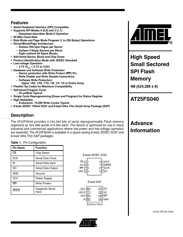
The AT25FS040 provides 4,194,304 bits of serial reprogrammable Flash memory organized as 524,288 words of 8 bits each. The device is optimized for use in many industrial and mercial applications where low-power and low-voltage operation are essential. The AT25FS040 is available in a space-saving 8-lead JEDEC SOIC and 8-lead Ultra Thin SAP packages. Table 1. Pin Configuration
Pin Name CS
SCK SI SO GND VCC WP
HOLD
Advance Information
Function
Chip Select Serial Data Clock Serial Data Input Serial Data Output Ground Power Supply
Write Protect
Suspends Serial Input
8-lead SAP
CS SO WP GND 1 2 3 4 8 7 6 5 VCC HOLD SCK SI
8-lead JEDEC SOIC
___
VCC 8 _____ HOLD 7 SCK 6 SI 5 1 2 3 4 CS SO ___ WP GND
Bottom...