AT45DB011
AT45DB011 is 1-Megabit 2.7-volt Only Serial DataFlash manufactured by Atmel.
- Part of the AT4-5DB comparator family.
- Part of the AT4-5DB comparator family.
Features
- Single 2.7V
- 3.6V Supply
- Serial Interface Architecture
- Page Program Operation
- -
- -
- -
- -
- -
- - Single Cycle Reprogram (Erase and Program)
- 512 Pages (264 Bytes/Page) Main Memory Optional Page and Block Erase Operations One 264-Byte SRAM Data Buffer Internal Program and Control Timer Fast Page Program Time
- 7 ms Typical 120 µs Typical Page to Buffer Transfer Time Low-Power Dissipation
- 4 m A Active Read Current Typical
- 2 µA CMOS Standby Current Typical 13 MHz Max Clock Frequency Hardware Data Protection Feature Serial Peripheral Interface (SPI) patible
- Modes 0 and 3 CMOS and TTL patible Inputs and Outputs mercial and Industrial Temperature Ranges
1-Megabit 2.7-volt Only Serial Data Flash® AT45DB011 Preliminary
Description
The AT45DB011 is a 2.7-volt only, serial interface Flash memory suitable for in-system reprogramming. Its 1,081,344 bits of memory are organized as 512 pages of 264 bytes each. In addition to the main memory, the AT45DB011 also contains one SRAM data buffer of 264 bytes. Unlike conventional Flash memories that are accessed randomly with multiple address lines and a parallel interface, the Data Flash uses a serial interface to sequentially access its data. The simple serial interface facilitates hard(continued)
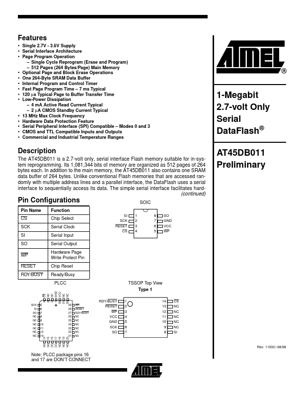
Pin Configurations
Pin Name CS SCK SI SO WP RESET RDY/BUSY Function Chip Select Serial Clock Serial Input Serial Output Hardware Page Write Protect Pin Chip Reset Ready/Busy PLCC
CS NC NC GND VCC NC NC
SOIC
SI SCK RESET CS 1 2 3 4 8 7 6 5 SO GND VCC WP
TSSOP Top View Type 1
RDY/BUSY RESET WP VCC GND SCK SO 1 2 3 4 5 6 7 14 13 12 11 10 9 8 CS NC NC NC NC NC SI
NC NC DC DC NC NC NC
14 15 16 17 18 19 20
SCK SI SO NC NC NC NC NC NC
5 6 7 8 9 10 11 12...