AT45DB080 Overview
Key Specifications
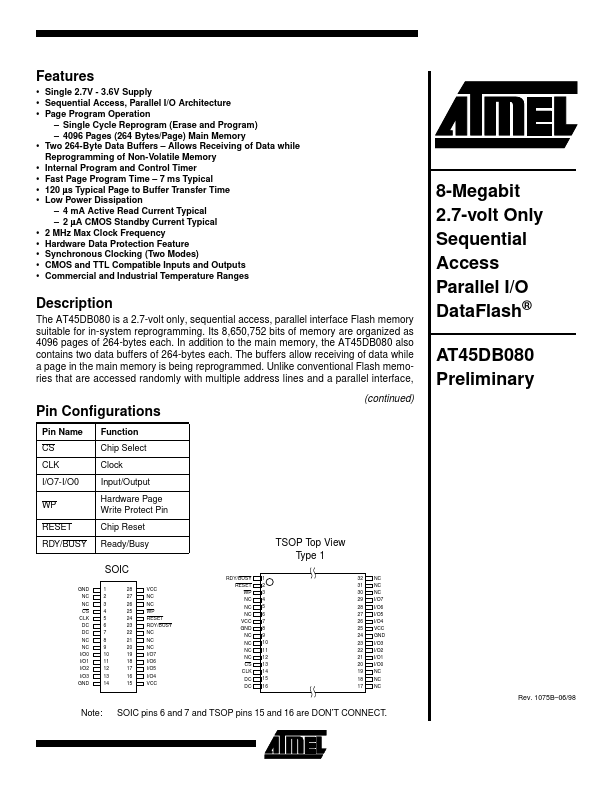
Package: TSOP
Description
The AT45DB080 is a 2.7-volt only, sequential access, parallel interface Flash memory suitable for in-system reprogramming. Its 8,650,752 bits of memory are organized as 4096 pages of 264-bytes each.
Key Features
- Sequential Access, Parallel I/O Architecture
- Page Program Operation