FCD4B14CCB
Features
- -
- -
- -
- -
- -
- -
Sensitive Layer Over a 0.8 µm CMOS Array Image Zone: 0.4 x 14 mm = 0.02" x 0.55" Image Array: 8 x 280 = 2240 pixels Pixel Pitch: 50 µm x 50 µm = 500 dpi Pixel Clock: up to 2 MHz Enabling up to 1780 Frames per Second Die Size: 1.7 x 17.3 mm Operating Voltage: 3V to 5.5V Naturally Protected Against ESD: > 16 k V Air Discharge Power Consumption: 20 m W at 3.3V, 1 MHz, 25°C Operating Temperature Range: 0°C to +70°C: C suffix Resistant to Abrasion: >1 Million Finger Sweeps Chip-On-Board (COB) package or 20-lead Ceramic DIP available for development, with Specific Protective Layer
Applications
- -
- -
- -
- -
- PDA (Access Control, Data Protection) Cellular Phones, Smart Phone (Access e-business) Notebook, PC-add on (Access Control, e-business) PIN Code Replacement Automated Teller Machine, POS Building Access Electronic Keys (Cars, Home,...) Portable Fingerprint Imaging for Law Enforcement TV Access
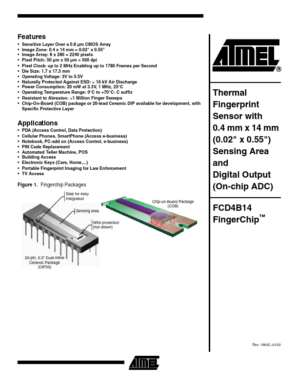
Figure 1. Fingerchip Packages
Step for easy integration...