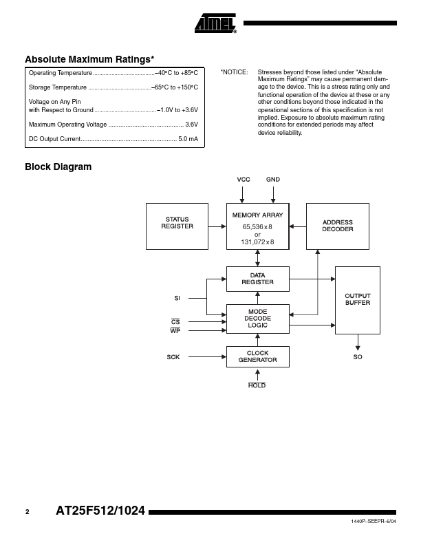
AT25F1024 Description
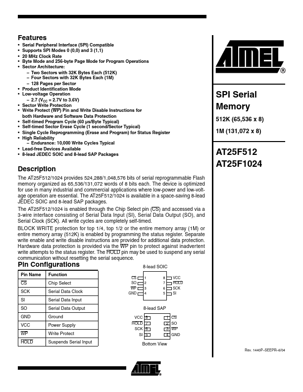
The device is optimized for use in many industrial and mercial applications where low-power and low-voltage operation are essential. The AT25F512/1024 is available in a space-saving 8-lead JEDEC SOIC and 8-lead SAP packages. The AT25F512/1024 is enabled through the Chip Select pin (CS) and accessed via a 3-wire interface consisting of Serial Data Input (SI), Serial Data Output (SO), and Serial Clock (SCK).
AT25F1024 Key Features
- Serial Peripheral Interface (SPI) patible
- Supports SPI Modes 0 (0,0) and 3 (1,1)
- 20 MHz Clock Rate
- Byte Mode and 256-byte Page Mode for Program Operations
- Sector Architecture
- Two Sectors with 32K Bytes Each (512K)
- Four Sectors with 32K Bytes Each (1M)
- 128 Pages per Sector
- Product Identification Mode
- Low-voltage Operation