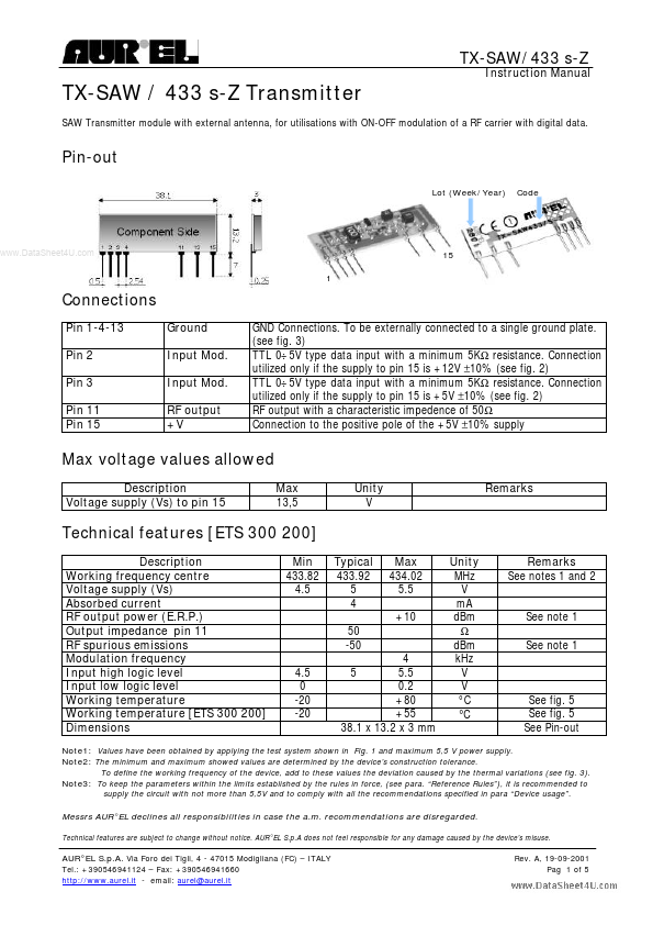
DESCRIPTION
Voltage supply (Vs) to pin 15 Max 13,5 Unity V Remarks Technical features [ETS 300 200] DESCRIPTION
Working frequency centre Voltage supply (Vs) Absorbed current RF output power (E.R.P.) Output impedance pin 11 RF spurious emissions Modulation frequency Input high logic level Input low logic level Working temperature Working temperature [ETS 300 200] Dimensions Min 433.82 4.5 Typical 433.92 5 4 50 -50 4.5 0 -20 -20 4 5 5.5 0.2 +80 +55 38.1 x 13.2 x 3 mm Max 434.02 5.5 +10 Unity MHz V mA dBm Ω dBm kHz V V °C °C Remarks See notes 1 and 2 See note 1 See note 1 See fig. 5 See fig. 5 See Pin-out Note1: Values have been obtained by applying the test system shown in Fig. 1 and maximum 5,5 V power supply. Note2: To define the working frequency of the device, add to these values the deviation caused by the thermal variations (see fig. 3). Note3: To keep the parameters within the limits established by the rules in force, (see para. “Reference Rules”), it is recommended to supply the circuit with not more than 5,5V and to comply with all the recommendations specified in para “Device usage”. AUREL