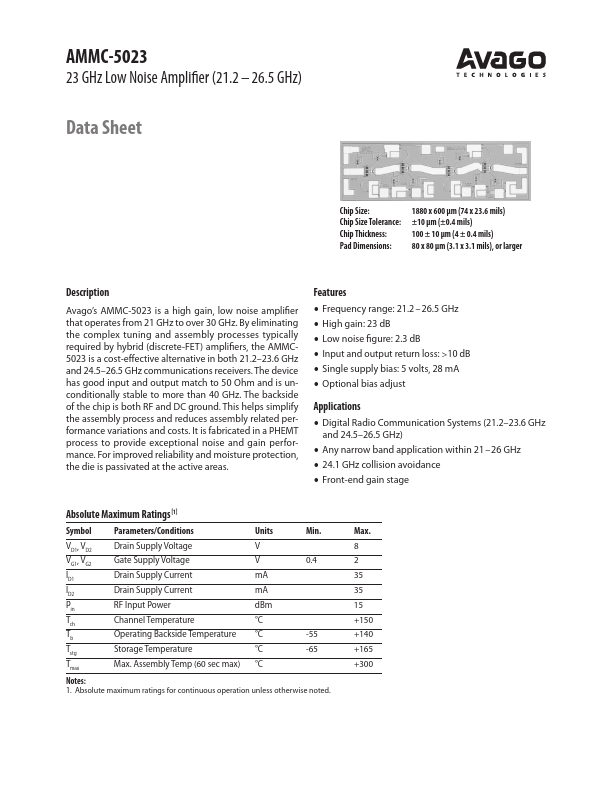
AMMC-5023
AMMC-5023 is Low Noise Amplifier manufactured by Avago Technologies.
Description
Avago’s AMMC-5023 is a high gain, low noise amplifier that operates from 21 GHz to over 30 GHz. By eliminating the plex tuning and assembly processes typically required by hybrid (discrete-FET) amplifiers, the AMMC5023 is a cost-effective alternative in both 21.2- 23.6 GHz and 24.5- 26.5 GHz munications receivers. The device has good input and output match to 50 Ohm and is unconditionally stable to more than 40 GHz. The backside of the chip is both RF and DC ground. This helps simplify the assembly process and reduces assembly related performance variations and costs. It is fabricated in a PHEMT process to provide exceptional noise and gain performance. For improved reliability and moisture protection, the die is passivated at the active areas.
Features
- Frequency range: 21.2
- 26.5 GHz
- High gain: 23 d B
- Low noise figure: 2.3 d B
- Input and output return loss: >10 d B
- Single supply bias: 5 volts, 28 m A
- Optional bias adjust
Applications
- Digital Radio munication Systems (21.2- 23.6 GHz and 24.5- 26.5 GHz)
- Any narrow band application within 21
- 26 GHz
- 24.1 GHz collision avoidance
- Front-end gain stage
Absolute Maximum Ratings [1]
Symbol Parameters/Conditions
Units
Min.
VD1, VD2 VG1, VG2 ID1 ID2 Pin Tch Tb Tstg Tmax
Drain Supply Voltage Gate Supply Voltage Drain Supply Current Drain Supply Current RF Input Power Channel Temperature Operating Backside Temperature Storage Temperature Max. Assembly Temp (60 sec max)
0.4 m A m A d Bm
°C
°C
-55
°C
-65
°C
Notes: 1. Absolute maximum ratings for continuous operation unless otherwise noted.
Max. 8 2 35 35 15 +150 +140 +165 +300
AMMC-5023 DC Specifications/Physical Properties[1]
Symbol Parameters and Test Conditions
Units Min. Typ. Max.
VD1, VD2 VG1, VG2 ID1, ID2 ID1+ID2 θch-b
Remended Drain Supply Voltage
Gate Supply Voltage[2] (VD1 ≤ VD1(max), VD2 ≤ VD2(max)) Input and Output Stage Drain Supply Current (VG1 = VG2 = Open, VD1 = VD2 = 5 V) Total Drain Supply Current...