MGA-81563
MGA-81563 is Amplifier manufactured by Avago Technologies.
Description
Avago’s MGA-81563 is an economical, easy-to-use Ga As MMIC amplifier that offers excellent power and low noise figure for applications from 0.1 to 6 GHz. Packaged in an ultra-miniature SOT-363 package, it requires half the board space of a SOT-143 package.
The output of the amplifier is matched to 50Ω (better than 2.1:1 VSWR) across the entire bandwidth. The input is partially matched to 50Ω (better than 2.5:1 VSWR) below 4 GHz and fully matched to 50Ω (better than 2:1 VSWR) above. A simple series inductor can be added to the input to improve the input match below 4 GHz. The amplifier allows a wide dynamic range by offering a 2.7 d B NF coupled with a +27 d Bm Output IP3.
The circuit uses state-of-the-art PHEMT technology with proven reliability. On-chip bias circuitry allows operation from a single +3 V power supply, while resistive feedback ensures stability (K>1) over all frequencies and temperatures.
Features x Lead-free Option Available x
+14.8 d Bm P at 2.0 GHz 1d B
+17 d Bm P at 2.0 GHz sat x Single +3V Supply x 2.8 d B Noise Figure at 2.0 GHz x 12.4 d B Gain at 2.0 GHz x Ultra-miniature Package x Unconditionally Stable
Applications x Buffer or Driver Amp for PCS, PHS, ISM, SAT and WLL Applications x High Dynamic Range LNA
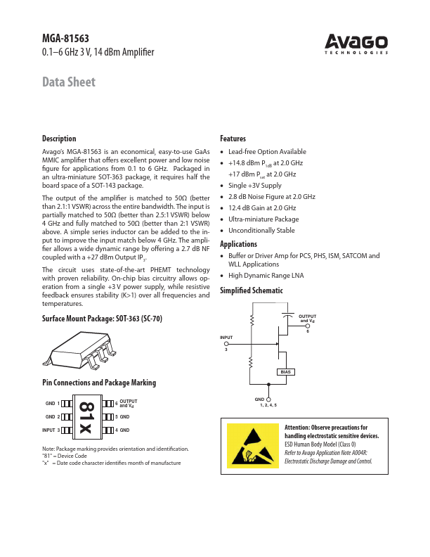
Simplified Schematic
Surface Mount Package: SOT-363 (SC-70)
INPUT
OUTPUT and Vd
Pin Connections and Package Marking
81x
GND 1 GND 2 INPUT 3
OUTPUT and Vd
5 GND
4 GND
Note: Package marking provides orientation and identification. "81" = Device Code "x" = Date code character identifies month of manufacture
BBIIAASS
GND 1, 2, 4, 5
Attention: Observe precautions for handling electrostatic sensitive devices. ESD Human Body Model (Class 0) Refer to Avago Application Note A004R: Electrostatic Discharge Damage and Control.
MGA-81563 Absolute Maximum Ratings
Symbol V d
V gd
V in
P in
T ch
T STG
Parameter Device Voltage, RF Output to Ground Device Voltage, Gate to Drain Range of RF Input Voltage to Ground CW RF...